SLVSDX0B October 2017 – November 2017 TPS23525
PRODUCTION DATA.
- 1 Features
- 2 Applications
- 3 Description
- 4 Revision History
- 5 Pin Configuration and Functions
- 6 Specifications
- 7 Parameter Measurement Information
- 8 Detailed Description
-
9 Application and Implementation
- 9.1 Application Information
- 9.2
Typical Application
- 9.2.1 Design Requirements
- 9.2.2
Detailed Design Procedure
- 9.2.2.1 Selecting RSNS
- 9.2.2.2 Selecting Soft Start Setting: CSS and CSS,VEE
- 9.2.2.3 Selecting VDS Switch Over Threshold
- 9.2.2.4 Timer Selection
- 9.2.2.5 MOSFET Selection and SOA Checks
- 9.2.2.6 Input Cap, Input TVS, and OR-ing FET selection
- 9.2.2.7 EMI Filter Consideration
- 9.2.2.8 Under Voltage and Over Voltage Settings
- 9.2.2.9 Choosing RVCC and CVCC
- 9.2.2.10 Power Good Interface to Downstream DC/DC
- 9.2.3 Application Curves
- 10Power Supply Recommendations
- 11Layout
- 12Device and Documentation Support
- 13Mechanical, Packaging, and Orderable Information
Package Options
Mechanical Data (Package|Pins)
- PW|16
Thermal pad, mechanical data (Package|Pins)
Orderable Information
11 Layout
11.1 Layout Guidelines
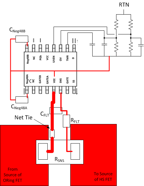
There are several things to keep in mind during layout of the TPS23525 circuit:
● The VEE and SNS pin need to have a Kelvin Sense connection to the sense resistor.
● The VEE trace carries current and needs to be thick and short in order to minimize IR drop and to avoid introducing current sensing error.
● It is recommended to use a net-tie to separate the power plane coming into the RSNS and the Kelvin connection to VEE.
● Connect the Neg48Vx filtering caps, UVEN resistor divider, OV resistor divider, and TMR cap to the "VEE" to insure maximum accuracy.
● The filtering caps on Neg48VB, Neg48VA, and SNS should be placed as close to the IC as possible.
11.2 Layout Example
 Figure 57. Layout Example