SLVS933D July 2009 – December 2020 TPS23753A
PRODUCTION DATA
- 1 Features
- 2 Applications
- 3 Description
- 4 Revision History
- 5 Product Information
- 6 Pin Configuration and Functions
- 7 Specifications
-
8 Detailed Description
- 8.1 Overview
- 8.2 Functional Block Diagram
- 8.3 Feature Description
- 8.4
Device Functional Modes
- 8.4.1 Threshold Voltages
- 8.4.2 PoE Start-Up Sequence
- 8.4.3 Detection
- 8.4.4 Hardware Classification
- 8.4.5 Maintain Power Signature (MPS)
- 8.4.6 TPS23753A Operation
- 8.4.7 Special Switching MOSFET Considerations
- 8.4.8 Thermal Considerations
- 8.4.9 FRS and Synchronization
- 8.4.10 Blanking – RBLNK
- 8.4.11 Current Slope Compensation
- 8.4.12 Adapter ORing
- 8.4.13 Protection
- 8.4.14 Frequency Dithering for Conducted Emissions Control
- 9 Application and Implementation
- 10Power Supply Recommendations
- 11Layout
- 12Device and Documentation Support
- 13Mechanical, Packaging, and Orderable Information
Package Options
Mechanical Data (Package|Pins)
- PW|14
Thermal pad, mechanical data (Package|Pins)
Orderable Information
8.4.11 Current Slope Compensation
Current-mode control requires addition of a compensation ramp to the sensed inductor (flyback transformer) current for stability at duty cycles near and over 50%. The TPS23753A has a maximum duty cycle limit of 78%, permitting the design of wide input-range flyback converters with a lower voltage stress on the output rectifiers. While the maximum duty cycle is 78%, converters may be designed that run at duty cycles well below this for a narrower, 36-V to 57-V range. The TPS23753A provides a fixed internal compensation ramp that suffices for most applications. RS (see Figure 8-8) may be used if the internally provided slope compensation is not enough. It works with ramp current (IPK = ISL-EX, approximately 40 μA) that flows out of the CS pin when the MOSFET is on. The IPK specification does not include the approximately 3-μA fixed current that flows out of the CS pin.
Most current-mode control papers and application notes define the slope values in terms of VPP/TS (peak ramp voltage / switching period); however, Electrical Characteristics: Controller Section Only specifies the slope peak (VSLOPE) based on the maximum duty cycle. Assuming that the desired slope, VSLOPE-D (in mV/period), is based on the full period, compute RS per Equation 7 where VSLOPE, DMAX, and ISL-EX are from Electrical Characteristics: Controller Section Only with voltages in mV, current in μA, and the duty cycle is unitless (for example, DMAX = 0.78).
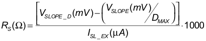
 Figure 8-8 Additional Slope Compensation
CS may be required if the presence of RS causes increased noise, due to adjacent signals like the gate drive, to appear at the CS pin. The TPS23753A has an internal pulldown on CS ( approximately 400 Ω maximum) while the MOSFET is OFF to reduce cycle-to-cycle carry-over voltage on CS.