SLVS933D July 2009 – December 2020 TPS23753A
PRODUCTION DATA
- 1 Features
- 2 Applications
- 3 Description
- 4 Revision History
- 5 Product Information
- 6 Pin Configuration and Functions
- 7 Specifications
-
8 Detailed Description
- 8.1 Overview
- 8.2 Functional Block Diagram
- 8.3 Feature Description
- 8.4
Device Functional Modes
- 8.4.1 Threshold Voltages
- 8.4.2 PoE Start-Up Sequence
- 8.4.3 Detection
- 8.4.4 Hardware Classification
- 8.4.5 Maintain Power Signature (MPS)
- 8.4.6 TPS23753A Operation
- 8.4.7 Special Switching MOSFET Considerations
- 8.4.8 Thermal Considerations
- 8.4.9 FRS and Synchronization
- 8.4.10 Blanking – RBLNK
- 8.4.11 Current Slope Compensation
- 8.4.12 Adapter ORing
- 8.4.13 Protection
- 8.4.14 Frequency Dithering for Conducted Emissions Control
- 9 Application and Implementation
- 10Power Supply Recommendations
- 11Layout
- 12Device and Documentation Support
- 13Mechanical, Packaging, and Orderable Information
Package Options
Mechanical Data (Package|Pins)
- PW|14
Thermal pad, mechanical data (Package|Pins)
Orderable Information
8.4.13 Protection
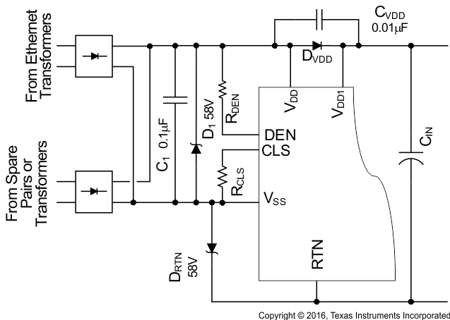
A TVS across the rectified PoE voltage per Figure 9-1 must be used. For general indoor applications, TI recommends an SMAJ58A or a part with equal to or better performance. If an adapter is connected from VDD1 to RTN, as in ORing option 2 above, voltage transients caused by the input cable inductance ringing with the internal PD capacitance can occur. Adequate capacitive filtering or a TVS must limit this voltage to be within the Absolute Maximum Ratings. Configurations that use DVDD as in Figure 8-10 may require additional protection against ESD transients that would turn DVDD off and force all the voltage to appear across the internal hotswap MOSFET. CVDD and DRTN per Figure 8-10 provide this additional protection.
 Figure 8-10 Additional Protection Against ESD
Outdoor applications require more extensive protection to lightning standards.