SLVS850A June 2008 – September 2023 TPS2551-Q1
PRODUCTION DATA
- 1
- 1 Features
- 2 Applications
- 3 Description
- 4 Revision History
- 5 Pin Configurations and Functions
- 6 Specifications
- 7 Parameter Measurement Information
- 8 Detailed Description
- 9 Application and Implementation
- 10Device and Documentation Support
- 11Mechanical, Packaging, and Orderable Information
Package Options
Mechanical Data (Package|Pins)
- DBV|6
Thermal pad, mechanical data (Package|Pins)
Orderable Information
6.6 Typical Characteristics
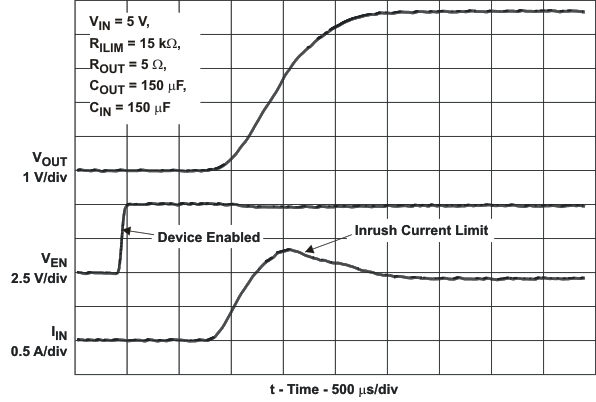 Figure 6-1 Turnon Delay and Rise Time
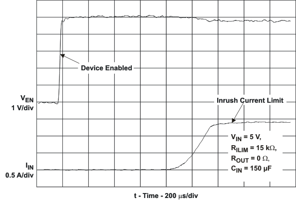 Figure 6-3 Device Enabled into Short-Circuit
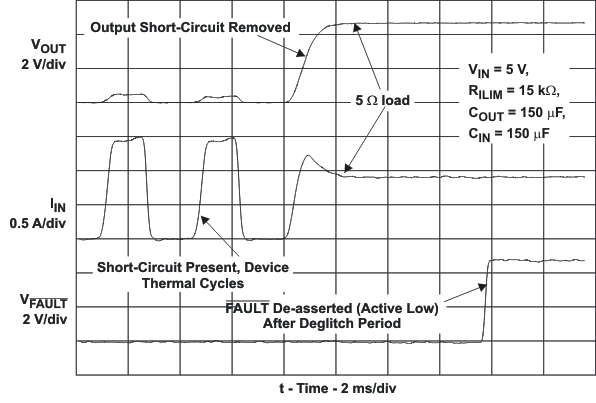 Figure 6-5 Short-Circuit to Full-Load Recovery Response
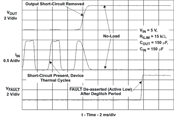 Figure 6-7 Short-Circuit to No-Load Recovery Response
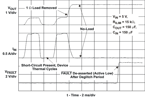 Figure 6-9 1Ω to
No Load Transient Response
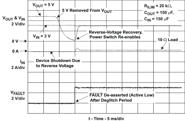 Figure 6-11 Reverse-Voltage Protection Recovery
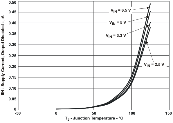 Figure 6-13 IIN – Supply Current, Output Disabled – μA
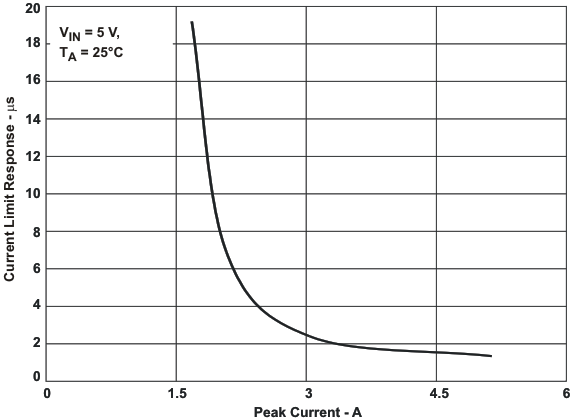 Figure 6-15 Current Limit Response – μs
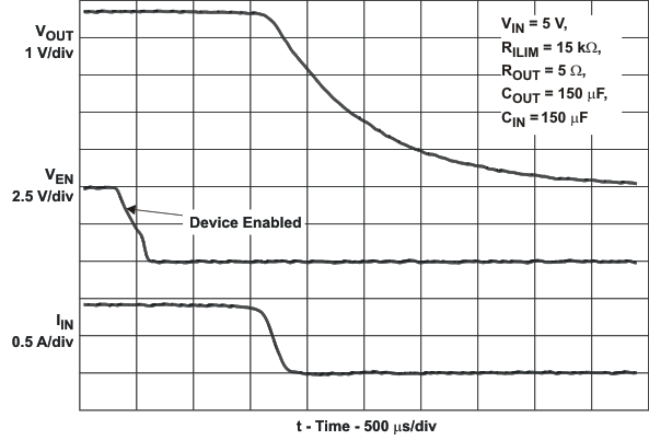 Figure 6-2 Turnoff Delay and Fall Time
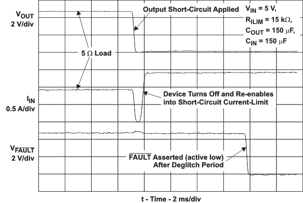 Figure 6-4 Full-Load to Short-Circuit Transient Response
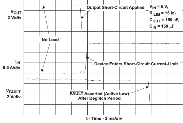 Figure 6-6 No-Load to Short-Circuit Transient Response
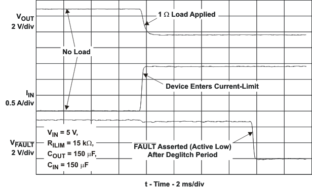 Figure 6-8 No
Load to 1Ω Transient Response
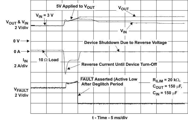 Figure 6-10 Reverse-Voltage Protection Response
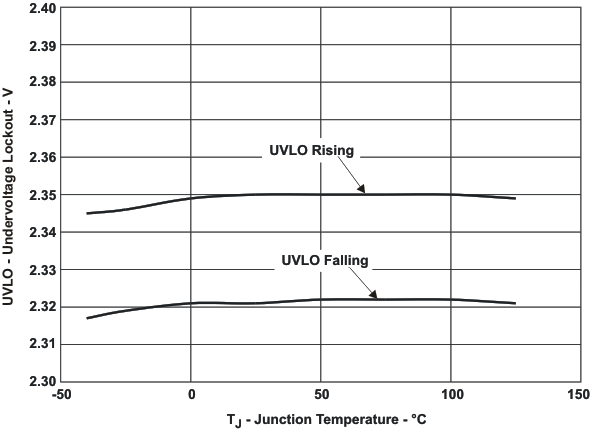 Figure 6-12 UVLO
– Undervoltage Lockout – V
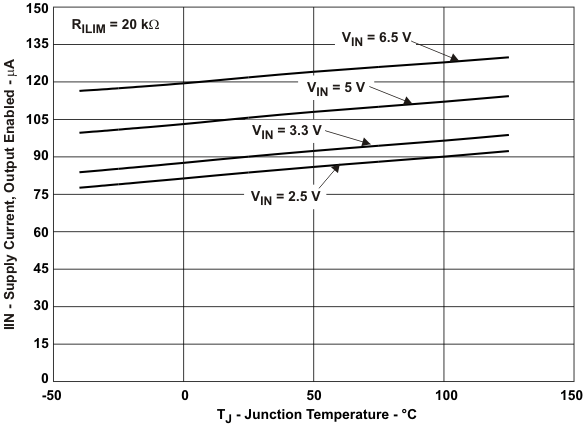 Figure 6-14 IIN – Supply Current, Output Enabled – μA
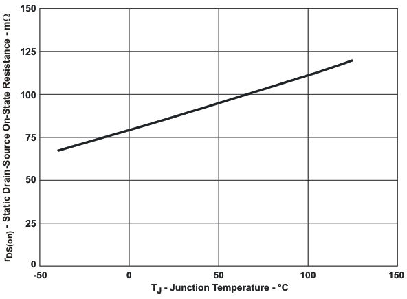 Figure 6-16 MOSFET rDS(on) Vs. Junction Temperature