SLVSE57C June 2017 – April 2018 TPS2595
PRODUCTION DATA.
- 1 Features
- 2 Applications
- 3 Description
- 4 Revision History
- 5 Device Comparison Table
- 6 Pin Configuration and Functions
- 7 Specifications
-
8 Detailed Description
- 8.1 Overview
- 8.2 Functional Block Diagram
- 8.3 Feature Description
- 8.4 Device Functional Modes
-
9 Application and Implementation
- 9.1 Application Information
- 9.2
Typical Application
- 9.2.1 Design Requirements
- 9.2.2 Detailed Design Procedure
- 9.2.3 Support Component Selection: CIN
- 9.2.4 Application Curves
- 9.2.5 Controlled Power Down (Quick Output Discharge) using TPS2595x5
- 9.2.6 Overvoltage Lockout using TPS259573
- 10Power Supply Recommendations
- 11Layout
- 12Device and Documentation Support
- 13Mechanical, Packaging, and Orderable Information
Package Options
Mechanical Data (Package|Pins)
- DSG|8
Thermal pad, mechanical data (Package|Pins)
- DSG|8
Orderable Information
8.4.3 Enable and Fault Pin Functional Mode 2: Multiple Devices, Self-Controlled
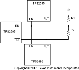
In this mode of operation, the devices are self-controlled (no host present). The EN and FLT pins are shorted together, and connected with up to three total devices as shown in Figure 55. In this configuration, when any one of the TPS2595xx devices detects a fault, it automatically disables the other TPS2595xx devices in the system.
NOTE
This configuration is only applicable to the Active High Enable variants TPS2595x0, TPS2595x1, TPS2595x5.
 Figure 55. Multiple Devices, Self-Controlled
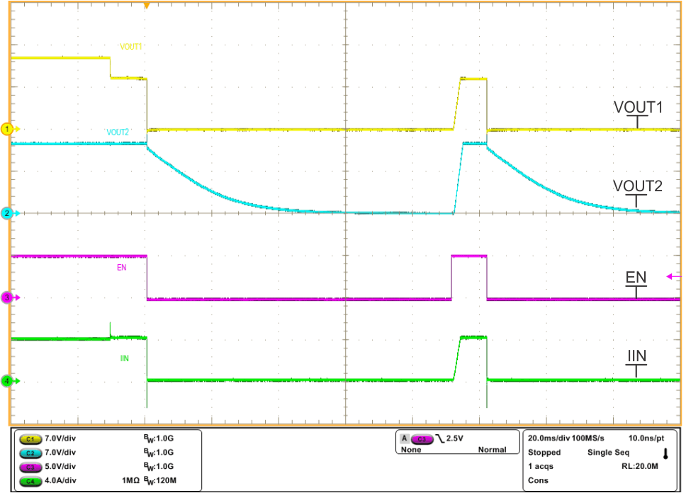
 Figure 56. TPS259541 Self-controlled Mode Response with Overload Fault on OUT1 Followed by Auto-retry with Persistent Fault
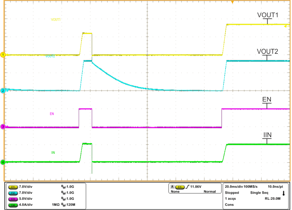
 Figure 57. TPS259541 Self-controlled Mode Response with Overload on OUT1 Followed by Recovery with Fault Removed