SLVSE42B October   2017  – September 2019 TPS27S100

PRODUCTION DATA.  

  1. Features
  2. Applications
  3. Description
    1.     Typical Application Schematic
  4. Revision History
  5. Pin Configuration and Functions
    1.     Pin Functions
  6. Specifications
    1. 6.1 Absolute Maximum Ratings
    2. 6.2 ESD Ratings
    3. 6.3 Recommended Operating Conditions
    4. 6.4 Thermal Information
    5. 6.5 Electrical Characteristics
    6. 6.6 Timing Requirements – Current Monitor Characteristics
    7. 6.7 Switching Characteristics
    8. 6.8 Typical Characteristics
  7. Detailed Description
    1. 7.1 Overview
    2. 7.2 Functional Block Diagram
    3. 7.3 Feature Description
      1. 7.3.1 Accurate Current Monitor
      2. 7.3.2 Adjustable Current Limit
      3. 7.3.3 Inductive-Load Switching-Off Clamp
      4. 7.3.4 Full Protections and Diagnostics
        1. 7.3.4.1 Short-to-GND and Overload Detection
        2. 7.3.4.2 Open-Load Detection
        3. 7.3.4.3 Short-to-Supply Detection
        4. 7.3.4.4 Thermal Fault Detection
        5. 7.3.4.5 UVLO Protection
        6. 7.3.4.6 Loss of GND Protection
        7. 7.3.4.7 Reverse Current Protection
        8. 7.3.4.8 Protection for MCU I/Os
    4. 7.4 Device Functional Modes
      1. 7.4.1 Working Mode
  8. Application and Implementation
    1. 8.1 Application Information
    2. 8.2 Typical Application
      1. 8.2.1 Design Requirements
      2. 8.2.2 Detailed Design Procedure
      3. 8.2.3 Application Curves
  9. Power Supply Recommendations
  10. 10Layout
    1. 10.1 Layout Guidelines
    2. 10.2 Layout Example
      1. 10.2.1 Without a GND Network
      2. 10.2.2 With a GND Network
  11. 11Device and Documentation Support
    1. 11.1 Receiving Notification of Documentation Updates
    2. 11.2 Community Resources
    3. 11.3 Trademarks
    4. 11.4 Electrostatic Discharge Caution
    5. 11.5 Glossary
  12. 12Mechanical, Packaging, and Orderable Information

Package Options

Mechanical Data (Package|Pins)
Thermal pad, mechanical data (Package|Pins)
Orderable Information

Application Curves

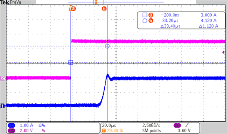
Figure 36 shows a an example of initial inrush or short-circuit current limit. Test conditions: EN is from low to high, load is resistive short-to-GND or with a 470-µF capacitive load, external current limit is 2 A. CH1 is the output current. CH3 is the EN step.

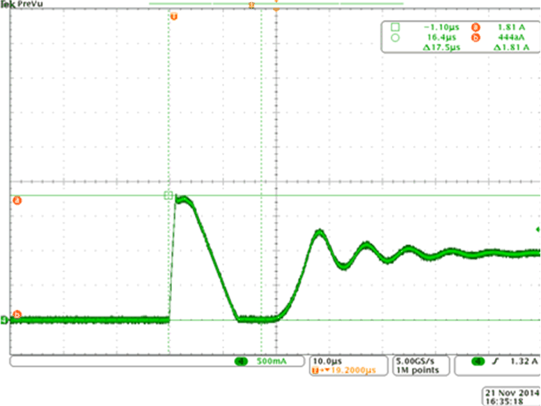
Figure 37 shows an example of current limit during hard short-circuit. Test conditions: EN is high, load is (5 µH + 100 mΩ), external current limit is 1 A. A short to GND suddenly happens.
TPS27S100 Graph1.gif
Figure 36. Initial Short-to-GND Waveform
TPS27S100 Graph2.gifFigure 37. Hard Short-to-GND Waveform