SLVSE42B October   2017  – September 2019 TPS27S100

PRODUCTION DATA.  

  1. Features
  2. Applications
  3. Description
    1.     Typical Application Schematic
  4. Revision History
  5. Pin Configuration and Functions
    1.     Pin Functions
  6. Specifications
    1. 6.1 Absolute Maximum Ratings
    2. 6.2 ESD Ratings
    3. 6.3 Recommended Operating Conditions
    4. 6.4 Thermal Information
    5. 6.5 Electrical Characteristics
    6. 6.6 Timing Requirements – Current Monitor Characteristics
    7. 6.7 Switching Characteristics
    8. 6.8 Typical Characteristics
  7. Detailed Description
    1. 7.1 Overview
    2. 7.2 Functional Block Diagram
    3. 7.3 Feature Description
      1. 7.3.1 Accurate Current Monitor
      2. 7.3.2 Adjustable Current Limit
      3. 7.3.3 Inductive-Load Switching-Off Clamp
      4. 7.3.4 Full Protections and Diagnostics
        1. 7.3.4.1 Short-to-GND and Overload Detection
        2. 7.3.4.2 Open-Load Detection
        3. 7.3.4.3 Short-to-Supply Detection
        4. 7.3.4.4 Thermal Fault Detection
        5. 7.3.4.5 UVLO Protection
        6. 7.3.4.6 Loss of GND Protection
        7. 7.3.4.7 Reverse Current Protection
        8. 7.3.4.8 Protection for MCU I/Os
    4. 7.4 Device Functional Modes
      1. 7.4.1 Working Mode
  8. Application and Implementation
    1. 8.1 Application Information
    2. 8.2 Typical Application
      1. 8.2.1 Design Requirements
      2. 8.2.2 Detailed Design Procedure
      3. 8.2.3 Application Curves
  9. Power Supply Recommendations
  10. 10Layout
    1. 10.1 Layout Guidelines
    2. 10.2 Layout Example
      1. 10.2.1 Without a GND Network
      2. 10.2.2 With a GND Network
  11. 11Device and Documentation Support
    1. 11.1 Receiving Notification of Documentation Updates
    2. 11.2 Community Resources
    3. 11.3 Trademarks
    4. 11.4 Electrostatic Discharge Caution
    5. 11.5 Glossary
  12. 12Mechanical, Packaging, and Orderable Information

Package Options

Mechanical Data (Package|Pins)
Thermal pad, mechanical data (Package|Pins)
Orderable Information

Typical Application

Figure 35 shows an example of how to design the external circuitry parameters.
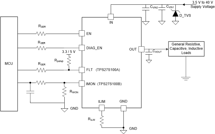
TPS27S100 Image1.gifFigure 35. Typical Application Circuitry

Table 3. Recommended External Components

COMPONENT TYPICAL VALUE PURPOSE
RSER 15 kΩ Protect microcontroller and device I/O pins
RIMON 1 kΩ Translate the sense current into sense voltage
CSNS 100 pF - 10 nF Low-pass filter for the ADC input
RILIM 0.82 kΩ Set current limit threshold
CVIN1/2 4.7 nF to Device GND Filtering of high frequency noise
220 nF to Module GND Stabilize the input supply and voltage spike suppression for surge transient immunity.
COUT 22 nF Immunity to ESD
DTVS 36V TVS diode Transient voltage clamp for surge transient immunity