SNVSBI5A July   2019  – September 2019 TPS3870-Q1

PRODUCTION DATA.  

  1. Features
  2. Applications
  3. Description
    1.     Device Images
      1.      Integrated Overvoltage Detection
      2.      Typical Overvoltage Accuracy Distribution
  4. Revision History
  5. Device Comparison Table
  6. Pin Configuration and Functions
    1.     Pin Functions
  7. Specifications
    1. 7.1 Absolute Maximum Ratings
    2. 7.2 ESD ratings
    3. 7.3 Recommended Operating Conditions
    4. 7.4 Thermal Information
    5. 7.5 Electrical Characteristics
    6. 7.6 Timing Requirements
    7. 7.7 Typical Characteristics
  8. Detailed Description
    1. 8.1 Overview
    2. 8.2 Functional Block Diagram
    3. 8.3 Feature Description
      1. 8.3.1 VDD
      2. 8.3.2 SENSE
      3. 8.3.3 RESET
      4. 8.3.4 Capacitor Time (CT)
      5. 8.3.5 Manual Reset (MR)
    4. 8.4 Device Functional Modes
      1. 8.4.1 Normal Operation (VDD > VDD(MIN))
      2. 8.4.2 Undervoltage Lockout (VPOR < VDD < UVLO)
      3. 8.4.3 Power-On Reset (VDD < VPOR)
  9. Application and Implementation
    1. 9.1 Application Information
      1. 9.1.1 Voltage Threshold Accuracy
      2. 9.1.2 CT Reset Time Delay
        1. 9.1.2.1 Factory-Programmed Reset Delay Timing
        2. 9.1.2.2 Programmable Reset Delay-Timing
      3. 9.1.3 RESET Latch Mode
      4. 9.1.4 Adjustable Voltage Thresholds
      5. 9.1.5 Immunity to SENSE Pin Voltage Transients
        1. 9.1.5.1 Hysteresis
    2. 9.2 Typical Application
      1. 9.2.1 Design 1: RESET Latch Mode
        1. 9.2.1.1 Design Requirements
        2. 9.2.1.2 Detailed Design Procedure
        3. 9.2.1.3 Application Curves
  10. 10Power Supply Recommendations
    1. 10.1 Power Supply Guidelines
  11. 11Layout
    1. 11.1 Layout Guidelines
    2. 11.2 Layout Example
  12. 12Device and Documentation Support
    1. 12.1 Device Nomenclature
    2. 12.2 Documentation Support
      1. 12.2.1 Evaluation Module
    3. 12.3 Receiving Notification of Documentation Updates
    4. 12.4 Support Resources
    5. 12.5 Trademarks
    6. 12.6 Electrostatic Discharge Caution
    7. 12.7 Glossary
  13. 13Mechanical, Packaging, and Orderable Information

Package Options

Mechanical Data (Package|Pins)
Thermal pad, mechanical data (Package|Pins)
Orderable Information

Design 1: RESET Latch Mode

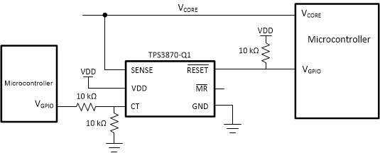
Another typical application for the TPS3870-Q1 is shown in Figure 25. The TPS3870-Q1 is used in a RESET latch output mode. In latch mode, once RESET driven logic low, it will stay low regardless of the sense voltage. If the RESET pin is low on start up, it will also stay low regardless of sense voltage.
TPS3870-Q1 LATCH-TPS3703-App-2.gifFigure 25. Window Voltage Monitoring with RESET Latch