SNVSBI5A July 2019 – September 2019 TPS3870-Q1
PRODUCTION DATA.
- 1 Features
- 2 Applications
- 3 Description
- 4 Revision History
- 5 Device Comparison Table
- 6 Pin Configuration and Functions
- 7 Specifications
- 8 Detailed Description
- 9 Application and Implementation
- 10Power Supply Recommendations
- 11Layout
- 12Device and Documentation Support
- 13Mechanical, Packaging, and Orderable Information
Package Options
Mechanical Data (Package|Pins)
- DSE|6
Thermal pad, mechanical data (Package|Pins)
Orderable Information
7.6 Timing Requirements
At 1.7 V ≤ VDD ≤ 5.5 V, CT = MR = Open, RESET Voltage (VRESET) = 10 kΩ to VDD, RESET load = 10 pF, and over the operating free-air temperature range of – 40°C to 125°C, unless otherwise noted. Typical values are at TJ = 25°C, typical conditions at VDD = 3.3 V.| MIN | NOM | MAX | UNIT | |||
|---|---|---|---|---|---|---|
| tD | Reset time delay, TPS3870J | CT = Open | 7 | 10 | 13 | ms |
| tD | Reset time delay, TPS3870J | CT = 10 kΩ to VDD | 140 | 200 | 260 | ms |
| tD | Reset time delay, TPS3870K | CT = Open | 0.7 | 1 | 1.3 | ms |
| tD | Reset time delay, TPS3870K | CT = 10 kΩ to VDD | 14 | 20 | 26 | ms |
| tD | Reset time delay, TPS3870L | CT = Open | 3.5 | 5 | 6.5 | ms |
| tD | Reset time delay, TPS3870L | CT = 10 kΩ to VDD | 70 | 100 | 130 | ms |
| tD | Reset time delay, TPS3870M | CT = 10 kΩ to VDD
CT = Open |
50 | µs | ||
| tPD | Propagation detect delay(1)(2) | 15 | 30 | µs | ||
| tR | Output rise time(1)(3) | 2.2 | µs | |||
| tF | Output fall time(1)(3) | 0.2 | µs | |||
| tSD | Startup delay(4) | 300 | µs | |||
| tGI (VIT+) | Glitch Immunity overvoltage VIT+(OV), 5% Overdrive(1) | 3.5 | µs | |||
| tGI (MR) | Glitch Immunity MR pin | 25 | ns | |||
| tPD (MR) | Propagation delay from MR low to assert RESET | 500 | ns | |||
| tMR_W | MR pin pulse width duration to assert RESET | 1 | µs | |||
| tD (MR) | MR reset time delay | tD | ms | |||
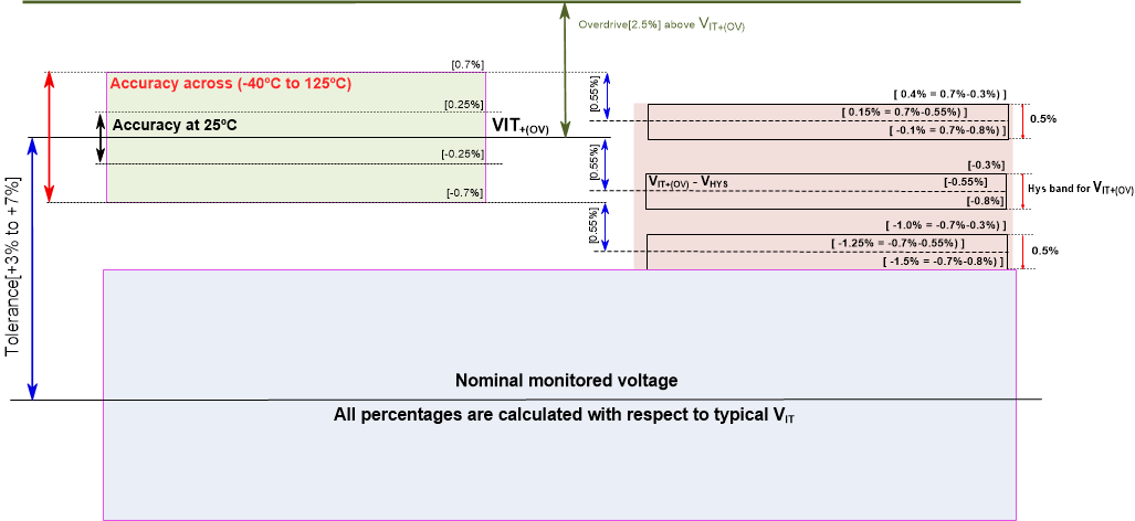
 Figure 1. Voltage Threshold and Hysteresis Accuracy
1. VDD = 2 V, RPU = 10 kΩ to VDD
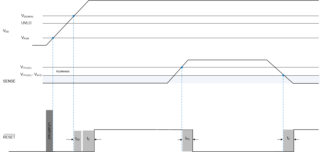
2. Variant M (time delay bypass) has a ~40 µs pulse at RESET pin during power up window, this is present only when the power cycle off time is longer than 10 seconds, this behavior will not occur if SENSE pin is within window of operation during VDD power up.
Figure 2. SENSE Timing Diagram