SNVSBI5A July   2019  – September 2019 TPS3870-Q1

PRODUCTION DATA.  

  1. Features
  2. Applications
  3. Description
    1.     Device Images
      1.      Integrated Overvoltage Detection
      2.      Typical Overvoltage Accuracy Distribution
  4. Revision History
  5. Device Comparison Table
  6. Pin Configuration and Functions
    1.     Pin Functions
  7. Specifications
    1. 7.1 Absolute Maximum Ratings
    2. 7.2 ESD ratings
    3. 7.3 Recommended Operating Conditions
    4. 7.4 Thermal Information
    5. 7.5 Electrical Characteristics
    6. 7.6 Timing Requirements
    7. 7.7 Typical Characteristics
  8. Detailed Description
    1. 8.1 Overview
    2. 8.2 Functional Block Diagram
    3. 8.3 Feature Description
      1. 8.3.1 VDD
      2. 8.3.2 SENSE
      3. 8.3.3 RESET
      4. 8.3.4 Capacitor Time (CT)
      5. 8.3.5 Manual Reset (MR)
    4. 8.4 Device Functional Modes
      1. 8.4.1 Normal Operation (VDD > VDD(MIN))
      2. 8.4.2 Undervoltage Lockout (VPOR < VDD < UVLO)
      3. 8.4.3 Power-On Reset (VDD < VPOR)
  9. Application and Implementation
    1. 9.1 Application Information
      1. 9.1.1 Voltage Threshold Accuracy
      2. 9.1.2 CT Reset Time Delay
        1. 9.1.2.1 Factory-Programmed Reset Delay Timing
        2. 9.1.2.2 Programmable Reset Delay-Timing
      3. 9.1.3 RESET Latch Mode
      4. 9.1.4 Adjustable Voltage Thresholds
      5. 9.1.5 Immunity to SENSE Pin Voltage Transients
        1. 9.1.5.1 Hysteresis
    2. 9.2 Typical Application
      1. 9.2.1 Design 1: RESET Latch Mode
        1. 9.2.1.1 Design Requirements
        2. 9.2.1.2 Detailed Design Procedure
        3. 9.2.1.3 Application Curves
  10. 10Power Supply Recommendations
    1. 10.1 Power Supply Guidelines
  11. 11Layout
    1. 11.1 Layout Guidelines
    2. 11.2 Layout Example
  12. 12Device and Documentation Support
    1. 12.1 Device Nomenclature
    2. 12.2 Documentation Support
      1. 12.2.1 Evaluation Module
    3. 12.3 Receiving Notification of Documentation Updates
    4. 12.4 Support Resources
    5. 12.5 Trademarks
    6. 12.6 Electrostatic Discharge Caution
    7. 12.7 Glossary
  13. 13Mechanical, Packaging, and Orderable Information

Package Options

Mechanical Data (Package|Pins)
Thermal pad, mechanical data (Package|Pins)
Orderable Information

RESET Latch Mode

The TPS3870-Q1 features a voltage latch mode on the RESET pin when connecting the CT pin to common ground . A pull-down resistor is recommended to limit current consumption of the system. In latch mode, if the RESET pin is low or triggers low, the pin will stay low regardless if VSENSE is within the acceptable voltage boundaries (VSENSE < VIT+(OV)). To unlatch the device provide a voltage to the CT pin that is greater than the CT pin comparator threshold voltage, VCT. The RESET pin will trigger high instantaneously without any reset delay. A voltage greater than 1.2 V to recommended to ensure a proper unlatch. Use a series resistance to limit current when an unlatch voltage is applied. For more information, Design 1: RESET Latch Mode gives an example of a typical latch application.

NOTE

At power up, the TPS3870-Q1 will be latched when CT is connected to GND. To ensure correct power up when using RESET latch mode, send a pulse to the CT pin greater than 1.2 V after tSD and SENSE is within the correct window of operation.
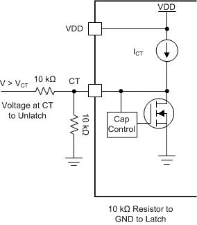
TPS3870-Q1 Latch_Application Information.gifFigure 22. RESET Latch Circuit