SNVSBI5A July   2019  – September 2019 TPS3870-Q1

PRODUCTION DATA.  

  1. Features
  2. Applications
  3. Description
    1.     Device Images
      1.      Integrated Overvoltage Detection
      2.      Typical Overvoltage Accuracy Distribution
  4. Revision History
  5. Device Comparison Table
  6. Pin Configuration and Functions
    1.     Pin Functions
  7. Specifications
    1. 7.1 Absolute Maximum Ratings
    2. 7.2 ESD ratings
    3. 7.3 Recommended Operating Conditions
    4. 7.4 Thermal Information
    5. 7.5 Electrical Characteristics
    6. 7.6 Timing Requirements
    7. 7.7 Typical Characteristics
  8. Detailed Description
    1. 8.1 Overview
    2. 8.2 Functional Block Diagram
    3. 8.3 Feature Description
      1. 8.3.1 VDD
      2. 8.3.2 SENSE
      3. 8.3.3 RESET
      4. 8.3.4 Capacitor Time (CT)
      5. 8.3.5 Manual Reset (MR)
    4. 8.4 Device Functional Modes
      1. 8.4.1 Normal Operation (VDD > VDD(MIN))
      2. 8.4.2 Undervoltage Lockout (VPOR < VDD < UVLO)
      3. 8.4.3 Power-On Reset (VDD < VPOR)
  9. Application and Implementation
    1. 9.1 Application Information
      1. 9.1.1 Voltage Threshold Accuracy
      2. 9.1.2 CT Reset Time Delay
        1. 9.1.2.1 Factory-Programmed Reset Delay Timing
        2. 9.1.2.2 Programmable Reset Delay-Timing
      3. 9.1.3 RESET Latch Mode
      4. 9.1.4 Adjustable Voltage Thresholds
      5. 9.1.5 Immunity to SENSE Pin Voltage Transients
        1. 9.1.5.1 Hysteresis
    2. 9.2 Typical Application
      1. 9.2.1 Design 1: RESET Latch Mode
        1. 9.2.1.1 Design Requirements
        2. 9.2.1.2 Detailed Design Procedure
        3. 9.2.1.3 Application Curves
  10. 10Power Supply Recommendations
    1. 10.1 Power Supply Guidelines
  11. 11Layout
    1. 11.1 Layout Guidelines
    2. 11.2 Layout Example
  12. 12Device and Documentation Support
    1. 12.1 Device Nomenclature
    2. 12.2 Documentation Support
      1. 12.2.1 Evaluation Module
    3. 12.3 Receiving Notification of Documentation Updates
    4. 12.4 Support Resources
    5. 12.5 Trademarks
    6. 12.6 Electrostatic Discharge Caution
    7. 12.7 Glossary
  13. 13Mechanical, Packaging, and Orderable Information

Package Options

Mechanical Data (Package|Pins)
Thermal pad, mechanical data (Package|Pins)
Orderable Information

Typical Characteristics

At TJ = 25°C, VDD = 3.3 V, and RPU = 10 kΩ, unless otherwise noted.
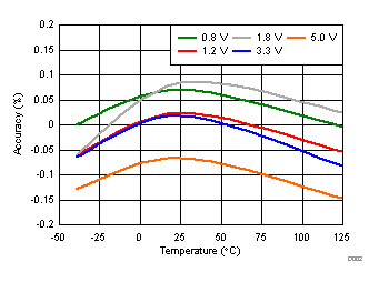
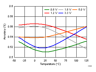
TPS3870-Q1 D002_SBVS344_VITp_ACC_VDD_3V3.gif
Tested across multiple voltage options
Figure 3. Overvoltage Accuracy vs Temperature
TPS3870-Q1 D006_SBVS344_VHYSp_ACC_VDD_3V3.gif
Tested across multiple voltage options
Figure 5. Overvoltage Hysteresis Voltage Accuracy vs Temperature
TPS3870-Q1 D008_SBVS344_Iq_RST_Low.gif
Output (RESET Pin) = Low
Figure 7. Supply Current vs Temperature
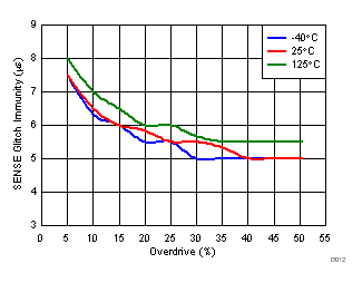
TPS3870-Q1 D012_SBVS344_TGI_VITp_VDD_5V5.gif
VDD = 5.5 V
Figure 9. SENSE Glitch Immunity (VIT+) vs Overdrive
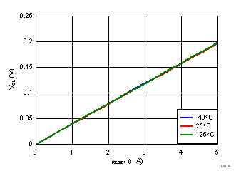
TPS3870-Q1 D014_SBVS344_VOL_IRST_5V5.gif
VDD = 5.5 V
Figure 11. Low-Level Output Voltage vs RESET current
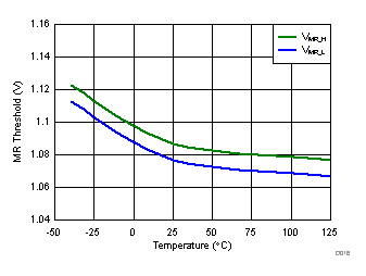
TPS3870-Q1 D016_SBVS344_MR_VDD_5V5.gif
VDD = 5.5 V
Figure 13. SET Threshold vs Temperature
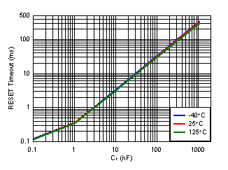
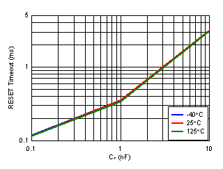
TPS3870-Q1 D018_SBVS344_CT_RESET_Delay.gif
Figure 15. RESET Timeout vs CT Capacitor
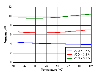
TPS3870-Q1 D020_SBVS344_tPD_Sense.gif
Figure 17. Detect Propagation Delay vs Temperature
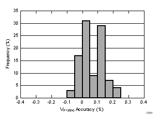
TPS3870-Q1 D004_SBVS344_Histo_VITp_ACC_VDD_3V3.gif
Figure 4. Overvoltage Accuracy Distribution
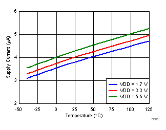
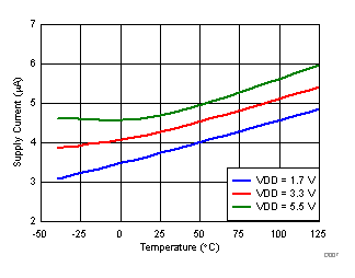
TPS3870-Q1 D007_SBVS344_Iq_RST_High.gif
Output (RESET Pin) = High
Figure 6. Supply Current vs Temperature
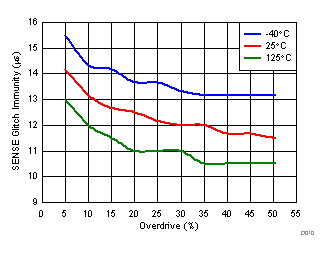
TPS3870-Q1 D010_SBVS344_TGI_VITp_VDD_1V7.gif
VDD = 1.7 V
Figure 8. SENSE Glitch Immunity (VIT+) vs Overdrive
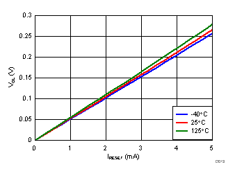
TPS3870-Q1 D013_SBVS344_VOL_IRST_1V7.gif
VDD = 1.7 V
Figure 10. Low-Level Output Voltage vs RESET current
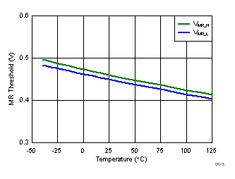
TPS3870-Q1 D015_SBVS344_MR_VDD_1V7.gif
VDD = 1.7 V
Figure 12. SET Threshold vs Temperature
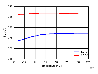
TPS3870-Q1 D017_SBVS344_ICTvsTemp.gif
Figure 14. CT Current vs CT value
TPS3870-Q1 D019_CT_Reset_Zoom.gif
Figure 16. Timeout vs CT Capacitor (0.1 to 10 nF)