SLUS658D July   2005  – June 2019 TPS40190

PRODUCTION DATA.  

  1. Features
  2. Applications
  3. Description
    1.     Device Images
      1.      Simplified Application Diagram
  4. Revision History
  5. Pin Configuration and Functions
    1.     Pin Functions
  6. Specifications
    1. 6.1 Absolute Maximum Ratings
    2. 6.2 Dissipation Ratings
    3. 6.3 Recommended Operating Conditions
    4. 6.4 Electrical Characteristics
    5. 6.5 Typical Characteristics
  7. Detailed Description
    1. 7.1 Overview
    2. 7.2 Functional Block Diagram
    3. 7.3 Feature Description
      1. 7.3.1 Internally Fixed Parameters
      2. 7.3.2 Output Short Circuit Protection
      3. 7.3.3 Enable Functionality
      4. 7.3.4 5-V Regulator
      5. 7.3.5 Startup Sequence and Timing
      6. 7.3.6 Prebias Outputs
  8. Application and Implementation
    1. 8.1 Typical Applications
  9. Device and Documentation Support
    1. 9.1 Documentation Support
      1. 9.1.1 Related Documentation
    2. 9.2 Receiving Notification of Documentation Updates
    3. 9.3 Community Resources
    4. 9.4 Trademarks
    5. 9.5 Electrostatic Discharge Caution
    6. 9.6 Glossary
  10. 10Mechanical, Packaging, and Orderable Information

Package Options

Refer to the PDF data sheet for device specific package drawings

Mechanical Data (Package|Pins)
  • DRC|10
Thermal pad, mechanical data (Package|Pins)
Orderable Information

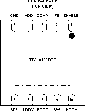
Pin Configuration and Functions

DRC Package
10-Pin VSON
Top View
TPS40190 po_lus658.gif

Pin Functions

PIN I/O DESCRIPTION
NO. NAME
1 ENABLE I Logic level input that starts or stops the controller from an external user command. A high level turns the controller on. This pin has a high-impedance internal pull-up integrated into the device. Because this pin is high impedance, a 10-nF capacitor to ground or an external pull-up resistor (100 kΩ) to VDD is recommended to avoid noise coupling to this pin.
2 FB I Inverting input to the error amplifier
3 COMP O Output of the error amplifier. Connecting a resistance from COMP to GND sets the output short circuit detection threshold. See applications information for details.
4 VDD I Power input to the controller
5 GND Common connection for the controller
6 BP5 O Output bypass for the internal regulator. Connect 4.7-μF capacitor from this pin to GND. Low power, low noise loads may be connected here if desired. The sum of the external load and the gate drive requirements must not exceed 40 mA. The regulator is turned off when the ENABLE pin is pulled low.
7 LDRV O Output to the rectifier FET gate
8 BOOT I Power supply for the flying high-side driver
9 SW I Sense line for the adaptive anti cross conduction circuitry. Serves as common connection for the flying high side FET driver
10 HDRV O Bootstrapped output for driving the gate of the high side N channel FET.