SLUS658D July 2005 – June 2019 TPS40190
PRODUCTION DATA.
- 1 Features
- 2 Applications
- 3 Description
- 4 Revision History
- 5 Pin Configuration and Functions
- 6 Specifications
- 7 Detailed Description
- 8 Application and Implementation
- 9 Device and Documentation Support
- 10Mechanical, Packaging, and Orderable Information
Package Options
Refer to the PDF data sheet for device specific package drawings
Mechanical Data (Package|Pins)
- DRC|10
Thermal pad, mechanical data (Package|Pins)
- DRC|10
Orderable Information
6.5 Typical Characteristics
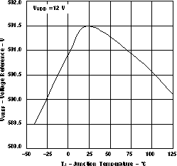 Figure 1. Reference Voltage vs Temperature
 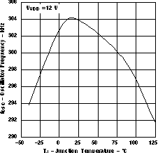 Figure 3. Oscillator Frequency vs Temperature
 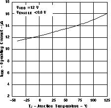 Figure 5. Operating Current vs Temperature
 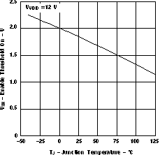 Figure 7. Enable Threshold On vs Temperature
 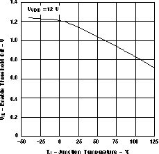 Figure 9. Enable Threshold Off vs Temperature
 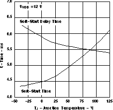 Figure 11. Soft Start Timing vs Temperature
 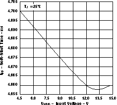 Figure 13. Soft Start Timing vs Input Voltage
 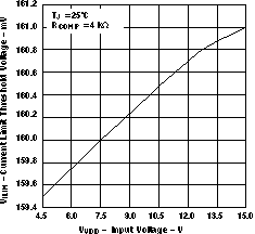 Figure 15. Current Limit Threshold vs Input Voltage
 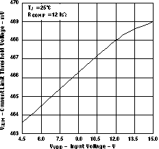 Figure 17. Current Limit Threshold vs Input Voltage
 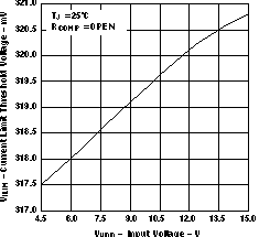 Figure 19. Current Limit Threshold vs Input Voltage
 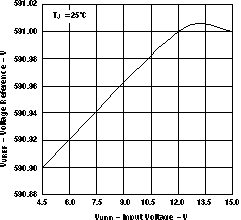 Figure 2. Reference Voltage vs Input Voltage
 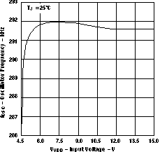 Figure 4. Oscillator Frequency vs Input Voltage
 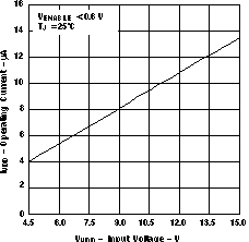 Figure 6. Operating Current vs Input Voltage
 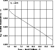 Figure 8. Enable Threshold On vs Input Voltage
 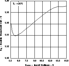 Figure 10. Enable Threshold Off vs Input Voltage
 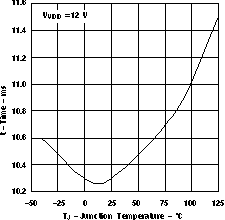 Figure 12. Total Startup Time vs Temperature
 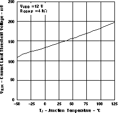 Figure 14. Current Limit Threshold vs Temperature
 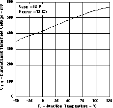 Figure 16. Current Limit Threshold vs Temperature
 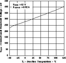 Figure 18. Current Limit Threshold vs Temperature
 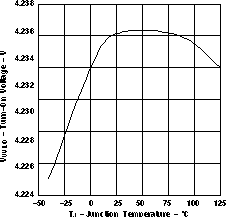 Figure 20. Undervoltage Lockout Turn On Voltage
vs Temperature