SLUS659G FEBRUARY 2006 – November 2014 TPS40200
PRODUCTION DATA.
- 1 Features
- 2 Applications
- 3 Description
- 4 Revision History
- 5 Pin Configuration and Functions
- 6 Specifications
- 7 Detailed Description
-
8 Application and Implementation
- 8.1 Application Information
- 8.2
Typical Application
- 8.2.1
Buck Regulator, 8 V to 12 V Input, 3.3 V to 5.0 V at 2.5-A Output
- 8.2.1.1 Design Requirements
- 8.2.1.2
Detailed Design Procedure
- 8.2.1.2.1 FET Selection Criteria
- 8.2.1.2.2 Rectifier Selection Criteria
- 8.2.1.2.3 Inductor Selection Criteria
- 8.2.1.2.4 Output Capacitance
- 8.2.1.2.5 Switching Frequency
- 8.2.1.2.6 Calculating the Overcurrent Threshold Level
- 8.2.1.2.7 Soft-Start Capacitor
- 8.2.1.2.8 Frequency Compensation
- 8.2.1.2.9 Printed Circuit Board Plots
- 8.2.1.3 Application Curves
- 8.2.2 18 V - 50 V Input, 16 V at 1-A Output
- 8.2.3 Wide Input Voltage Led Constant Current Driver
- 8.2.1
Buck Regulator, 8 V to 12 V Input, 3.3 V to 5.0 V at 2.5-A Output
- 9 Power Supply Recommendations
- 10Layout
- 11Device and Documentation Support
- 12Mechanical, Packaging, and Orderable Information
Package Options
Refer to the PDF data sheet for device specific package drawings
Mechanical Data (Package|Pins)
- D|8
- DRB|8
Thermal pad, mechanical data (Package|Pins)
- DRB|8
Orderable Information
1 Features
- Input Voltage Range 4.5 V to 52 V
- Output Voltage (700 mV to 90% VIN)
- 200-mA Internal P-channel FET Driver
- Voltage Feed-Forward Compensation
- Undervoltage Lockout
- Programmable Fixed-Frequency (between 35 kHz and 500 kHz) Operation
- Programmable Short-Circuit Protection
- Hiccup Overcurrent Fault Recovery
- Programmable Closed-Loop Soft-Start
- 700 mV 1% Reference Voltage
- External Synchronization
- Small 8-Pin SOIC (D) and VSON (DRB) Packages
2 Applications
- Industrial Control
- Distributed Power Systems
- DSL/Cable Modems
- Scanners
- Telecom
3 Description
The TPS40200 is a flexible, non-synchronous controller with a built-in 200-mA driver for P-channel FETs. The circuit operates with inputs up to 52 V with a power-saving feature that turns off driver current once the external FET has been fully turned on. This feature extends the flexibility of the device, allowing it to operate with an input voltage up to 52 V without dissipating excessive power. The circuit operates with voltage-mode feedback and has feed-forward input voltage compensation that responds instantly to input voltage change. The integral 700-mV reference is trimmed to 2%, providing the means to accurately control low voltages. The TPS40200 is available in an 8-pin SOIC and an 8-pin VSON package and supports many of the features of more complex controllers. Clock frequency, soft-start, and overcurrent limits are each easily programmed by a single, external component. The part has undervoltage lockout, and can be easily synchronized to other controllers or a system clock to satisfy sequencing and/or noise-reduction requirements.
Device Information(1)
| PART NUMBER | PACKAGE | BODY SIZE (NOM) |
|---|---|---|
| TPS40200 | VSON (8) | 3.00 mm x 3.00 mm |
| SOIC (8) | 4.90 mm x 3.90 mm |
- For all available packages, see the orderable addendum at the end of the datasheet.
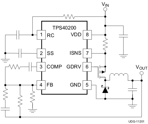
Simplified Schematic
Efficiency vs Output Current
