SLUS659G FEBRUARY 2006 – November 2014 TPS40200
PRODUCTION DATA.
- 1 Features
- 2 Applications
- 3 Description
- 4 Revision History
- 5 Pin Configuration and Functions
- 6 Specifications
- 7 Detailed Description
-
8 Application and Implementation
- 8.1 Application Information
- 8.2
Typical Application
- 8.2.1
Buck Regulator, 8 V to 12 V Input, 3.3 V to 5.0 V at 2.5-A Output
- 8.2.1.1 Design Requirements
- 8.2.1.2
Detailed Design Procedure
- 8.2.1.2.1 FET Selection Criteria
- 8.2.1.2.2 Rectifier Selection Criteria
- 8.2.1.2.3 Inductor Selection Criteria
- 8.2.1.2.4 Output Capacitance
- 8.2.1.2.5 Switching Frequency
- 8.2.1.2.6 Calculating the Overcurrent Threshold Level
- 8.2.1.2.7 Soft-Start Capacitor
- 8.2.1.2.8 Frequency Compensation
- 8.2.1.2.9 Printed Circuit Board Plots
- 8.2.1.3 Application Curves
- 8.2.2 18 V - 50 V Input, 16 V at 1-A Output
- 8.2.3 Wide Input Voltage Led Constant Current Driver
- 8.2.1
Buck Regulator, 8 V to 12 V Input, 3.3 V to 5.0 V at 2.5-A Output
- 9 Power Supply Recommendations
- 10Layout
- 11Device and Documentation Support
- 12Mechanical, Packaging, and Orderable Information
Package Options
Refer to the PDF data sheet for device specific package drawings
Mechanical Data (Package|Pins)
- D|8
- DRB|8
Thermal pad, mechanical data (Package|Pins)
- DRB|8
Orderable Information
8 Application and Implementation
NOTE
Information in the following applications sections is not part of the TI component specification, and TI does not warrant its accuracy or completeness. TI’s customers are responsible for determining suitability of components for their purposes. Customers should validate and test their design implementation to confirm system functionality.
8.1 Application Information
The TPS40200 is a 4.5-V to 52-V buck controller with an integrated gate driver for a high-side p-channel MOSFET. This device is typically used to convert a higher DC voltage to a lower DC voltage with a maximum output current set by an external current sense resistor. In higher current applications, the maximum output current can also be limited by the thermal performance of the external MOSFET and rectifying diode switch. Use the following design procedure to select external components for the TPS40200. The design procedure illustrates the design of a typical buck regulator with the TPS40200.
8.2 Typical Application
8.2.1 Buck Regulator, 8 V to 12 V Input, 3.3 V to 5.0 V at 2.5-A Output
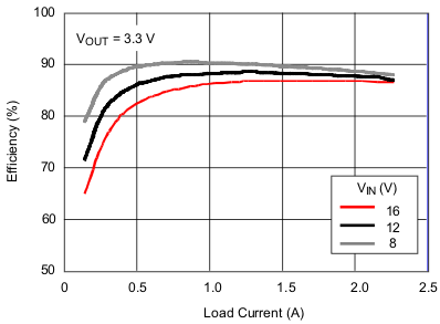
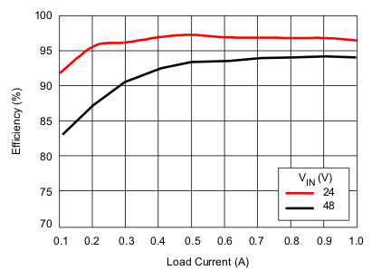
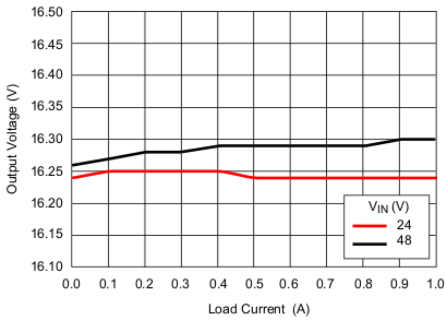
The buck regulator design shown in Figure 31 shows the use of the TPS40200. It delivers 2.5 A at either 3.3 V or 5.0 V as selected by a single feedback resistor. It achieves approximately 90% efficiency at 3.3 V and 94% at 5.0 V. A discussion of design tradeoffs and methodology is included to serve as a guide to the successful design of buck converters using the TPS40200.
The Bill of Materials for this application is given in Table 2. The efficiency and load regulation from boards built from this design are shown in Figure 42 and Figure 43.
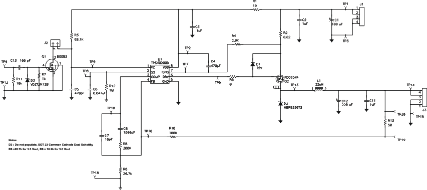 Figure 31. 8 V to 16 VIN Step-Down Buck Converter
8.2.1.1 Design Requirements
Table 1. Design Parameters
| PARAMETER | TEST CONDITION | MIN | NOM | MAX | UNIT | |
|---|---|---|---|---|---|---|
| VIN | Input Voltage | 8 | 12 | 16 | V | |
| VOUT | Output Voltage | IOUT = 2.5 A | 3.2 | 3.3 | 3.4(1) | V |
| Line Regulation | ± 0.2 % VOUT | 3.293 | 3.300 | 3.307 | V | |
| Load Regulation | ± 0.2% VOUT | 3.293 | 3.300 | 3.307 | V | |
| VOUT | Output Voltage | IOUT at 2.5 A | 4.85 | 5.0 | 5.150(1) | V |
| Line Regulation | ± 0.2% × VOUT | 4.99 | 5.00 | 5.01 | V | |
| Load Regulation | ± 0.2% × VOUT | 4.99 | 5.00 | 5.01 | V | |
| VRIPPLE | Output ripple voltage | At maximum output current | 60 | mV | ||
| VOVER | Output overshoot | For 2.5 A load transient from 2.5 A to 0.25 A | 100 | mV | ||
| VUNDER | Output undershoot | For 2.5 A load transient from 0.25 A to 2.5 A | 60 | mV | ||
| IOUT | Output Current | 0.125 | 2.500 | A | ||
| ISCP | Short circuit current trip point | 3.75 | 5.00 | A | ||
| Efficiency | At nominal input voltage and maximum output current | 90% | ||||
| FS | Switching frequency | 300 | kHz | |||
8.2.1.2 Detailed Design Procedure
8.2.1.2.1 FET Selection Criteria
- The maximum input voltage for this application is 16 V. Switching the inductor causes overshoot voltages that can equal the input voltage. Since the RDS(on) of the FET rises with breakdown voltage, select a FET with as low a breakdown voltage as possible. In this case, a 30-V FET was selected.
- The selection of a power FET size requires knowing both the switching losses and DC losses in the application. AC losses are all frequency dependent and directly related to device capacitances and device size. On the other hand, DC losses are inversely related to device size. The result is an optimum where the two types of losses are equal. Since device size is proportional to RDS(on), begin by selecting a device with an RDS(on) that results in a small loss of power relative to package thermal capability and overall efficiency objectives.
- In this application, the efficiency target is 90% and the output power 8.25 W. This gives a total power-loss budget of 0.916 W. Total FET losses must be small relative to this number.
The DC conduction loss in the FET is given by: PDC = Irms2 × RDS(on)
The RMS current is given by:
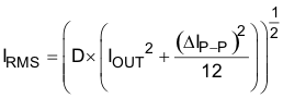
Where
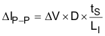
ΔV = VIN – VOUT –(DCR + RDS(on)) × IOUT
RDS(on) is the FET on-state resistance
DCR is the inductor DC resistance
D is the duty cycle
tS = the reciprocal of the switching frequency
Using the values in this example, the DC power loss is 129 mW. The remaining FET losses are as follows:
- PSW is the power dissipated while switching the FET on and off
- PGATE is the power dissipated driving the FET gate capacitance
- PCOSS is the power switching the FET output capacitance
The total power dissipated by the FET is the sum of these contributions.

The P-channel FET used in this application is a FDC654P with the following characteristics:
| tRISE = 13 × 10–9 | COSS = 83 × 10–12 | |
| tFALL = 6 × 10⁻⁹ | QG = 9 nC | |
| RDS(on) = 0.1 Ω | VGATE= 1.9 V | |
| QGD = 1.2 × 10⁻⁹ | QGS = 1.0 × 10⁻⁹ |
Using these device characteristics and Equation 10:
where  and
and  are the switching times for the power FET.
The gate current, IG = QG × fS = 2.7 mA
The sum of the switching losses is 34 mW, and is comparable to the 129-mW DC losses. At added expense, a slightly larger FET is better because the DC loss drops and the AC losses increase, with both moving toward the optimum point of equal losses.
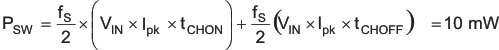
8.2.1.2.2 Rectifier Selection Criteria
- Rectifier Breakdown Voltage
- Diode Size
The rectifier has to withstand the maximum input voltage which in this case is 16 V. To allow for switching transients which can approach the switching voltage a 30-V rectifier was selected.
The importance of power losses from the Schottky rectifier D2 is determined by the duty cycle. For a low duty cycle application, the rectifier is conducting most of the time, and the current that flows through it times its forward drop can be the largest component of loss in the entire controller. In this application, the duty cycle ranges from 20% to 40%, which in the worst case means that the diode is conducting 80% of the time. Where efficiency is of paramount importance, choose a diode with a minimum of forward drop. In more cost sensitive applications, size may be reduced to the point of the thermal limitations of the diode package.
The device in this application is large relative to the current required by the application. In a more cost sensitive application, a smaller diode in a less-expensive package will provide a less-efficient but appropriate solution
The device used has the following characteristics:
- Vf = 0.3 V at 3 A
- Ct = 300 pF (Ct = the effective reverse voltage capacitance of the synchronous rectifier, D2).
The two components of the losses from the diode D2 are:
Where
D = the duty cycle
IRIPPLE is the ripple current
IOUT is the output current
VF is the forward voltage
PCOND is the conduction power loss
The switching capacitance of this diode adds an AC loss, given by:
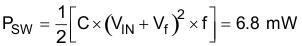
This additional loss raises the total loss to: 660 mW.
At an output voltage of 3.3 V, the application runs at a nominal duty cycle of 27%, and the diode is conducting 72.5% of the time. As the output voltage is moved up to 5 V, the on-time increases to 46% and the diode is conducting only 54% of the time during each clock cycle. This change in duty cycle proportionately reduces the conduction power losses in the diode. This reduction may be expressed as
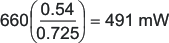 for a savings in power of 660 – 491 = 169 mW.
To illustrate the relevance of this power savings we measured the full load module Efficiency for this application at 3.3 V and 5 V. The 5-V output efficiency is 92% vs. 89% for the 3.3 V design. This difference in efficiency represents a 456 mW reduction in losses between the two conditions. This 169 mW power-loss reduction in the rectifier represents 37% of the difference.
8.2.1.2.3 Inductor Selection Criteria
The P-channel FET driver facilitates switching the power FET at a high frequency. This, in turn, enables the use of smaller, less-expensive inductors as illustrated in this 300 kHz application. Ferrite, with its good high frequency properties, is the material of choice. Several manufacturers provide catalogs with inductor saturation currents, inductance values, and LSRs (internal resistance) for their various-sized ferrites.
In this application, the device must deliver a maximum current of 2.5 A. This requires that the output inductor’s saturation current be above 2.5 A plus ½ the ripple current caused during inductor switching. The value of the inductor determines this ripple current. A low value of inductance has a higher ripple current that contributes to ripple voltage across the resistance of the output capacitors. The advantages of a low inductance are a higher transient response, lower DCR, a higher saturation current, and a smaller, less expensive part. Too low an inductor however, leads to higher peak currents which ultimately are bounded by the overcurrent limit set to protect the output FET or by output ripple voltage. Fortunately, with low ESR Ceramic capacitors on the output, the resulting ripple voltage for relatively high ripple currents can be small.
For example, a single 1-μF, 1206 size, 6.3-V, ceramic capacitor has an internal resistance of 2 Ω at 1 MHz. For this 2.5-A application, a 10% ripple current of 0.25 A produces a 50-mV ripple voltage. This ripple voltage may be further reduced by additional parallel capacitors.
The other bound on inductance is the minimum current at which the controller enters discontinuous conduction. At this point, Inductor current is zero. The minimum output current for this application is specified at 0.125 A. This average current is 1/2 the peak current that must develop during a minimum on time. The conditions for minimum on time are high line and low load.
Using:
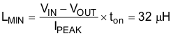
Where
VIN = 16 V
VOUT = 3.3 V
IPEAK = 0.25 A
tON = 0.686 μs
tON is given by 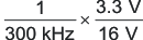
The inductor used in the circuit is the closest standard value of 33 μH. This is the minimum inductance that can be used in the converter to deliver the minimum current while maintaining continuous conduction.
8.2.1.2.4 Output Capacitance
In order to satisfy the output voltage over and under shoot specifications there must be enough output capacitance to keep the output voltage within the specified voltage limits during load current steps.
In a situation where a full load of 2.5 A within the specified voltage limits is suddenly removed, the output capacitor must absorb energy stored in the output inductor. This condition may be described by realizing that the energy in the stored in the inductor must be suddenly absorbed by the output capacitance. This energy relationship is written as:
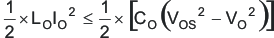
Where
VOS is the allowed over-shoot voltage above the output voltage
LO is the inductance
IO is the output current
CO is the output capacitance
VO is the output voltage
In this application, the worst case load step is 2.25 A and the allowed overshoot is 100 mV. With a 33 μH output inductor, this implies an output capacitance of 249 μF for a 3.3 V output and 165 μF for a 5 V output..
When the load increases from minimum to full load the output capacitor must deliver current to the load. The worst case is for a minimum on time that occurs at 16 V in and 3.3 VOUT and minimum load. This corresponds to an off time of (1 – 0.2 ) times the period 3.3 μs and is the worst case time before the inductor can start supplying current. This situation may be represented by:
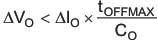
Where
ΔVO is the undershoot specification of 60 mV
ΔIO is the load current step
tOFF(max) is the maximum off time
This condition produces a requirement of 100 μF for the output capacitance. The larger of these two requirements becomes the minimum value of output capacitance.
The ripple current develops a voltage across the ESR of the output capacitance, so another requirement on this component is it ESR be small relative to the ripple voltage specification.
8.2.1.2.5 Switching Frequency
The TPS40200 has a built-in, 8-V, 200-mA, P-channel FET driver output that facilitates using P-channel switching FETs A clock frequency of 300 kHz is chosen as a switching frequency that represents a compromise between a high-frequency that allows the use of smaller capacitors and inductors but one that is not so high as to cause excessive transistor switching losses. As previously discussed, an optimum frequency can be selected by picking a value where the DC and switching losses are equal.
The frequency is set by using the design formula given in the FET Selection Criteria section.
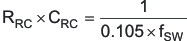
Where
RRC is the timing resistor value in Ω
RRC = 68.1 kΩ
CRC is the timing capacitor value in F
C5 = 470 pF
fSW is the desired switching frequency in Hz
fSW = 297 kHz.
At a worst case of 16 V, the timing resistor draws about 250 μA which is well below the 750 μA maximum which the circuit can pull down.
8.2.1.2.6 Calculating the Overcurrent Threshold Level
The current limit in the TSP40200 is triggered by a comparator with a 100-mV offset whose inputs are connected across a current-sense resistor between VIN and the source of the high-side switching FET. When current in this resistor develops more than 100 mV, the comparator trips and terminates the output gate drive.
In this application, the current-limit resistor is set by the peak output stage current which consists of the maximum load current plus ½ the ripple current. In this case, we have 2.5 + 0.125 = 2.625 A. To accommodate tolerances a 25% margin is added giving a 3.25 A peak current. Using the equation below then yields a value for RILIM of 0.03 Ω.
Current sensing in a switching environment requires attention to both circuit board traces and noise pick up. In the design shown a small RC filter has been added to the circuit to prevent switching noise from tripping the current sense comparator. The requirements of this filter are board-dependent, but with the layout used in this application, no unreasonable overcurrent is observed.
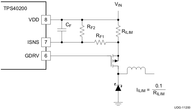 Figure 32. Overcurrent Trip Circuit for RF2 Open
8.2.1.2.7 Soft-Start Capacitor
The soft-start interval is given (in pF) by the following equation:
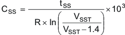
Where
R is an internal 105-kΩ charging resistor
VIN is the input voltage up to 8 V where the charging voltage is internally clamped to 8 V maximum
VOS = 700 mV, and because the input voltage is 12 V, VSST = 8 V.
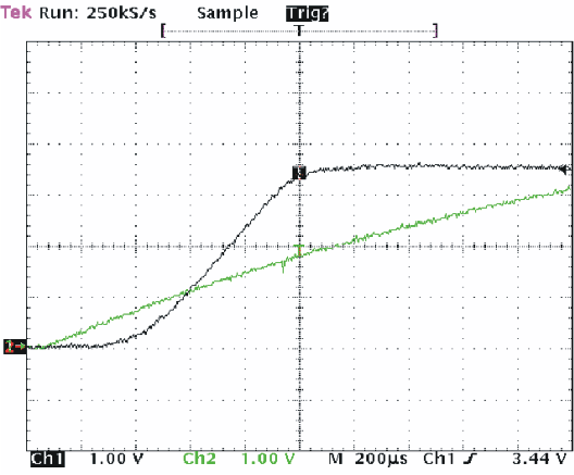
The oscilloscope picture below shows the expected delay at the output (middle trace) until the soft-start node (bottom trace) reaches 700 mV. At this point, the output rises following the exponential rise of the soft-start capacitor voltage until the soft-start capacitor reaches 1.4 V and the internal 700-mV reference takes over. This total time is approximately 1 ms, which agrees with the calculated value of 0.95 ms where the soft-start capacitance is 0.047 μF.
8.2.1.2.8 Frequency Compensation
The four elements that determine the system overall response are discussed below The gain of the error amplifier (KEA) is the first of there elements. Its output develops a control voltage which is the input to the PWM.
The TPS40200 has a unique modulator that scales the peak to peak amplitude of the PWM ramp to be 0.1 times the value of the input voltage. Since modulator gain is given by VIN divided by VRAMP, the modulator gain is 10 and is constant at 10 (20 dB) over the entire specified input voltage range.
The last two elements that affect system gain are the transfer characteristic of the output LC filter and the feedback network from the output to the input to the error amplifier.
These four elements maybe expressed by the following expression that represents the system transfer function as shown in Figure 34.

Where
KFB is the output voltage setting divider
KEA is the error amplifier feedback
KPWM is the modulator gain
XLC is the filter transfer function
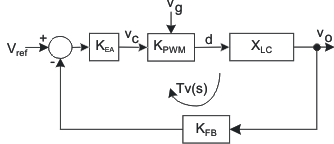 Figure 34. Control Loop
Figure 35 shows the feedback network used in this application. This is a Type II compensation network which gives a combination of good transient response and phase boost for good stability. This type of compensation has a pole at the origin causing a –20dB/decade (–1) slope followed by a zero that causes a region of flat gain followed by a final pole that returns the gain slope to –1. The bode plot in Figure 36 shows the effect of these poles and zeros.
The procedure for setting up the compensation network is as follows:
- Determine the break frequency of the output capacitor.
- Select a zero frequency well below this break frequency.
- From the gain bandwidth of the error amplifier select a crossover frequency where the amplifier gain is large relative to expected closed loop gain
- Select a second zero well above the crossover frequency, that returns the gain slope to a –1 slope.
- Calculate the required gain for the amplifier at crossover.
The frequency response of this converter is largely determined by two poles that arise from the LC output filter and a higher frequency zero caused by the ESR of the output capacitance. The poles from the output filter cause a –40 dB/decade roll off with a phase shift approaching 180 degrees followed by the output capacitor zero that reduced the roll off to –20 dB and gives a phase boost back toward 90 degrees. In other nomenclature, this is a –2 slope followed by a –1 slope. The two zeros in the compensation network act to cancel the double pole from the output filter The compensation network’s two poles produce a region where the error amplifier is flat and can be set to a gain such that the overall gain of the system is zero dB. This region is set so that it brackets the system crossover frequency.
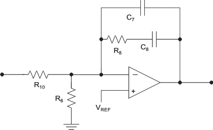 Figure 35. Error Amplifier Feedback Elements
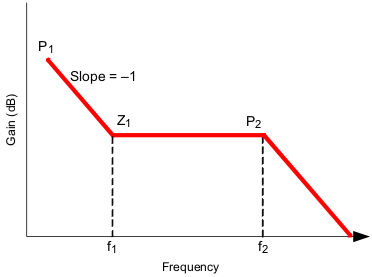 Figure 36. Error Amplifier Bode Plot
In order to properly compensate this system, it is necessary to know the frequencies of its poles and zeros.
8.2.1.2.8.1 Step 1
The break frequency of the output capacitor is given by:
Where
COUT = the output capacitor, 220 μF
RESR = the ESR of the capacitors
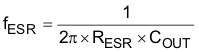
Because of the ESR of the output capacitor, the output LC filter has a single-pole response above the 1.8-kHz break frequency of the output capacitor and its ESR. This simplifies compensation since the system becomes essentially a single pole system.
8.2.1.2.8.2 Step 2
The first zero is place well below the 1.8-kHz break frequency of the output capacitor and its ESR. The phase boost from this zero is shown in Figure 38.
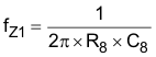
Where
R8 = 300 kΩ
C8 = 1500 pF
fZ1 = 354 Hz
8.2.1.2.8.3 Step 3
From its minimum gain bandwidth product of 1.5 MHz, and knowing it has a 20 dB/decade roll off, the open-loop gain of the error amplifier is 33 dB at 35 kHz. This approximate frequency is chosen for a crossover frequency to keep the amplifier gain contribution to the overall system gain small, as well as following the convention of placing the crossover frequency between 1/6 to 1/10 the 300 kHz switching frequency.
8.2.1.2.8.4 Step 4
The second pole is placed well above the 35 kHz crossover frequency.
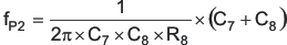
Where
R8 = 300 kΩ
C7 = 10 pF
C8 = 1500 pF
fP2 = 53 kHz
8.2.1.2.8.5 Step 5
Calculate the gain elements in the system to determine the gain required by the error amplifier to make the over all gain 0 dB at 35 kHz.
The total gain around the voltage feedback loop is:
Where
KFB is the output voltage setting divider
KEA is the error amplifier feedback
KPWM is the modulator gain
XLC is the filter transfer function
With reference to the graphic below, the output filter's transfer characteristic XLC (S) can be estimated by the following:
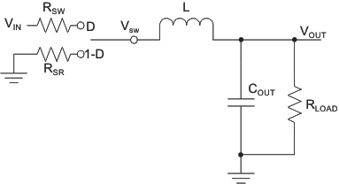 Figure 37. Output Filter Analysis
Where
ZOUT is the parallel combination of output capacitor(s) and the load
RSW is the RDS(on) of the switching FET plus the current-sense resistor
RSR is the resistance of the synchronous rectifier
D is the duty cycle estimated as 3.3 / 12 = 0.27
To evaluate XLC(S) at 35 kHz use the following:
- ZOUT(s) at 35 kHz, which is dominated by the output capacitor's ESR; estimated to be 400 mΩ
- ZL(s) at 35 kHz is 7.25 Ω
- RSW = 0.95 mΩ, including the RLIM resistance
- RSR = 100 mΩ
Using these numbers, XLC(S) = 0.04 or –27.9 dB.
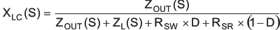
The feedback network has a gain to the error amplifier given by:

Where
for 3.3 VOUT, R6 = 26.7 kΩ
Using the values in this application, Kfb = 11.4 dB.
The modulator has a gain of 10 that is flat to well beyond 35 kHz, so KPWM = 20 dB.
To achieve 0 db overall gain, the amplifier and feedback gain must be set to –7.9 dB (20 dB – 27.9dB).
The amplifier gain, including the feedback gain, Kfb, can be approximated by this expression:
Where
Zfs is the parallel combination of C7 in parallel with the sum of R8 and the impedance of C8.
AVOLis the open-loop gain of the error amplifier at 35 kHz, which is 44.6 dB or 33 dB.
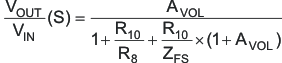
Figure 38 shows the result of the compensation. The crossover frequency is 35 kHz and the phase margin is 45°. The response of the system is dominated by the ESR of the output capacitor and is exploited to produce an essentially single-pole system with simple compensation.
 Figure 38. Overall System Gain and Phase Response
Figure 38 also shows the phase boost that gives the system a crossover phase margin of 47°.
The bill of materials for this application is shown below. The efficiency and load regulation from boards built from this design are shown in the following two figures. Gerber PCB layout files and additional application information are available from the factory.
Table 2. Bill of Materials, Buck Regulator, 12 V to 3.3 V and 5.0 V
| REF. DES. | VALUE | DESCRIPTION | SIZE | MFR. | PART NUMBER |
|---|---|---|---|---|---|
| C1 | 100 μF | Capacitor, Aluminum, SM, 25V, 0.3 Ω | 8 x 10 mm | Sanyo | 20SVP100M |
| C12 | 220 μF | Capacitor, Aluminum, SM, 6.3V, 0.4 Ω | 8 x 6.2 mm | Panasonic | EEVFC0J221P |
| C13 | 100 pF | Capacitor, Ceramic, 50V, [COG], [20%] | 603 | muRata | Std. |
| C3 | 0.1 pF | Capacitor, Ceramic, 50V, [X7R], [20%] | 603 | muRata | Std. |
| C2, C11 | 1 μF | Capacitor, Ceramic, 50V, [X7R], [20%] | 603 | muRata | Std. |
| C4, C5 | 470 pF | Capacitor, Ceramic, 50V, [X7R], [20%] | 603 | muRata | Std. |
| C6 | 0.047 μF | Capacitor, Ceramic, 50V, [X7R], [20%] | 603 | muRata | Std. |
| C7 | 10 pF | Capacitor, Ceramic, 50V, [COG], [20%] | 603 | muRata | Std. |
| C8 | 1500 pF | Capacitor, Ceramic, 50V, [X7R], [20%] | 603 | muRata | Std. |
| D1 | 12 V | Diode, Zener, 12-V, 350mW | SOT23 | Diodes, Inc. | BZX84C12T |
| D2 | Diode, Schottky, 30A, 30V | SMC | On Semi | MBRS330T3 | |
| D3 | 12 V | Diode Zener 12V 5mA | VMD2 | Rohm | VDZT2R12B |
| J1,J3 | Terminal Block 4-Pin 15A 5.1 mm | 0.8 x 0.35 | OST | ED2227 | |
| J2 | Header, 2-pin, 100 mil spacing, (36-pin strip) | 0.100 x 2 | Sullins | PTC36SAAN | |
| L1 | 33 μH | Inductor, SMT, 3.2A, .039 Ω | 12.5 x 12.5 mm | TDK | SLF12575T330M3R2PF |
| PCB | 2 Layer PCB 2 Ounce Cu | 1.4 x 2.12 x 0.062 | HPA164 | ||
| Q1 | Trans, N-Chan Enhancement Switching, 50mA | SOT-143B | Phillips | BSS83 | |
| Q2 | MOSFET, P-ch, 30V, 3.6A, 75mΩ | SuperSOT-6 | Fairchild | FDC654P | |
| U1 | IC, Low Cost Non-Sync Buck Controller | SO-8 | TI | TPS40200D | |
| R1 | 10 Ω | Resistor, Chip, 1/16W, 1% | 603 | Std. | Std. |
| R10 | 100 kΩ | Resistor, Chip, , 1/16W, 1% | 603 | Std. | Std. |
| R11 | 10 kΩ | Resistor, Chip, 1/16W, 1% | 603 | Std. | Std. |
| R12 | 1 MΩ | Resistor, Chip, 1/16W, 1% | 603 | Std. | Std. |
| R13 | 49.9 Ω | Resistor, Chip, 1/16W, 1% | 603 | Std. | Std. |
| R2 | 0.02 Ω | Resistor, Chip, ½ W, 5% | 2010 | Std. | Std. |
| R3 | 68.1 kΩ | Resistor, Chip, 1/16W, 1% | 603 | Std. | Std. |
| R4 | 2.0 kΩ | Resistor, Chip, 1/16W, 1% | 603 | Std. | Std. |
| R5 | 0 Ω | Resistor, Chip, 1/16W, 1% | 603 | Std. | Std. |
| R6 | 26.7 kΩ | Resistor, Chip, 1/16W, 1% | 603 | Std. | Std. |
| R7 | 1.0 kΩ | Resistor, Chip, 1/16W, 1% | 603 | Std. | Std. |
| R8 | 300 kΩ | Resistor, Chip, 1/16W, 1% | 603 | Std. | Std. |
8.2.1.2.9 Printed Circuit Board Plots
The following figures Figure 39 through Figure 41 show the design of the TPS40200EVM-001 printed circuit board. The design uses 2-layer, 2-oz copper and is 1.4” x 2.3” in size. All components are mounted on the top side to allow the user to easily view, probe, and evaluate the TPS40200 control IC in a practical application. Moving components to both sides of the printed circuit board (PCB) or using additional internal layers can offer additional size reduction for space constrained applications.
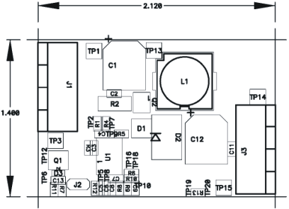 Figure 39. TPS40200EVM-001 Component Placement (Viewed from Top)
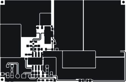 Figure 40. TPS40200EVM-001 Top Copper (Viewed from Top)
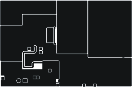 Figure 41. TPS40200EVM-001 Bottom Copper (X-Ray View from Top)
8.2.1.3 Application Curves

8.2.2 18 V - 50 V Input, 16 V at 1-A Output
This is an example of using the TPS40200 in a higher voltage application. The output voltage is 16 V at 1 A with an 18 V to 50 V input. Some of the test results are shown below.
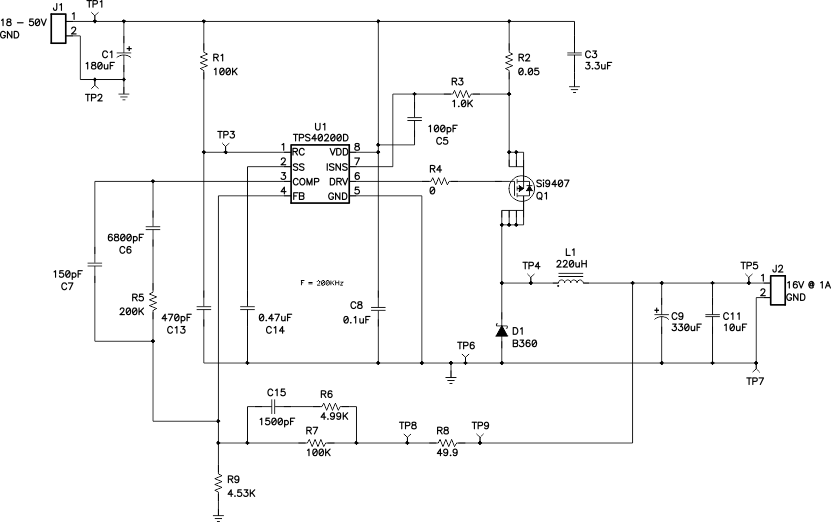 Figure 44. Buck Converter. VIN = 18 V to 50 V; VOUT = 16 V @ 1 A
8.2.2.1 Design Requirements
Table 3. Design Parameters
| PARAMETER | MIN | NOM | MAX | UNIT | |
|---|---|---|---|---|---|
| VIN | Input Voltage | 18 | 50 | V | |
| VOUT | Output Voltage | 16 | |||
| IOUT | Output Current | 1 | A | ||
| ISCP | Short circuit current trip point | 2 | |||
| FS | Switching Frequency | 200 | kHz | ||
8.2.2.2 Detailed Design Procedures
Using the design parameters stated in Table 3, follow the detailed design procedures listed under Detailed Design Procedure.
8.2.2.3 Application Curves
8.2.3 Wide Input Voltage Led Constant Current Driver
This application uses the TPS40200 as a buck controller that drives a string of LED diodes. The feedback point for this circuit is a sense resistor in series with this string. The low 0.7 V reference minimizes power wasted in this resistor, and maintains the LED current at a value given by 0.7/RSENSE. As the input voltage is varied, the duty cycle changes to maintain the LED current at a constant value so that the light intensity does not change with large input voltage variations.
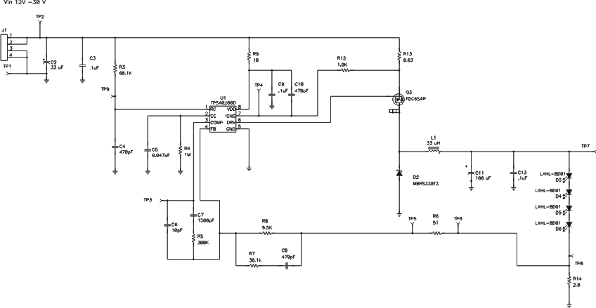 Figure 47. Wide-Input Voltage Range LED Driver
8.2.3.1 Design Requirements
Table 4. Design Parameters
| PARAMETER | MIN | NOM | MAX | UNIT | ||
|---|---|---|---|---|---|---|
| VIN | Input Voltage | 12 | 30 | V | ||
| ILED | Output Voltage | 0.25 | A | A | ||
| ISCP | Short circuit current trip point | 3.3 | A | |||
| FS | Switching Frequency | 300 | kHz | |||
8.2.3.2 Detailed Design Procedures
Using the design parameters stated in Table 4, follow the detailed design procedures listed under Detailed Design Procedure.
8.2.3.3 Application Curve
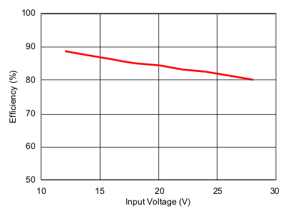 Figure 48. Efficiency vs Input Voltage