SLUS659G FEBRUARY 2006 – November 2014 TPS40200
PRODUCTION DATA.
- 1 Features
- 2 Applications
- 3 Description
- 4 Revision History
- 5 Pin Configuration and Functions
- 6 Specifications
- 7 Detailed Description
-
8 Application and Implementation
- 8.1 Application Information
- 8.2
Typical Application
- 8.2.1
Buck Regulator, 8 V to 12 V Input, 3.3 V to 5.0 V at 2.5-A Output
- 8.2.1.1 Design Requirements
- 8.2.1.2
Detailed Design Procedure
- 8.2.1.2.1 FET Selection Criteria
- 8.2.1.2.2 Rectifier Selection Criteria
- 8.2.1.2.3 Inductor Selection Criteria
- 8.2.1.2.4 Output Capacitance
- 8.2.1.2.5 Switching Frequency
- 8.2.1.2.6 Calculating the Overcurrent Threshold Level
- 8.2.1.2.7 Soft-Start Capacitor
- 8.2.1.2.8 Frequency Compensation
- 8.2.1.2.9 Printed Circuit Board Plots
- 8.2.1.3 Application Curves
- 8.2.2 18 V - 50 V Input, 16 V at 1-A Output
- 8.2.3 Wide Input Voltage Led Constant Current Driver
- 8.2.1
Buck Regulator, 8 V to 12 V Input, 3.3 V to 5.0 V at 2.5-A Output
- 9 Power Supply Recommendations
- 10Layout
- 11Device and Documentation Support
- 12Mechanical, Packaging, and Orderable Information
Package Options
Refer to the PDF data sheet for device specific package drawings
Mechanical Data (Package|Pins)
- D|8
- DRB|8
Thermal pad, mechanical data (Package|Pins)
- DRB|8
Orderable Information
6 Specifications
6.1 Absolute Maximum Ratings
over operating free-air temperature range (unless otherwise noted) (1)| MIN | MAX | UNIT | |||
|---|---|---|---|---|---|
| Input voltage range | VDD , ISNS | –0.3 | 52 | V | |
| RC, FB | –0.3 | 5.5 | |||
| SS | –0.3 | 9.0 | |||
| Output voltage range | COMP | –0.3 | 9.0 | V | |
| GDRV | VIN –10 | VIN | |||
| TJ | Operating Junction Temperature | –40 | 125 | °C | |
| Lead temperature 1,6 mm (1/16 inch) from case for 10 seconds | 260 | ||||
(1) Stresses beyond those listed under Absolute Maximum Ratings may cause permanent damage to the device. These are stress ratings only, which do not imply functional operation of the device at these or any other conditions beyond those indicated under Recommended Operating Conditions. Exposure to absolute-maximum-rated conditions for extended periods may affect device reliability.
6.2 Handling Ratings
| MIN | MAX | UNIT | |||
|---|---|---|---|---|---|
| Tstg | Storage temperature range | –55 | 150 | °C | |
| V(ESD) | Electrostatic discharge | Human body model (HBM), per ANSI/ESDA/JEDEC JS-001, all pins(1) | –1500 | 1500 | V |
| Charged device model (CDM), per JEDEC specification JESD22-C101, all pins(2) | –1500 | 1500 | |||
(1) JEDEC document JEP155 states that 500 V HBM allows safe manufacturing with a standard ESD control process.
(2) JEDEC document JEP157 states that 250 V CDM allows safe manufacturing with a standard ESD control process.
6.3 Recommended Operating Conditions
over operating free-air temperature range (unless otherwise noted)| MIN | MAX | UNIT | ||
|---|---|---|---|---|
| VDD | Input voltage | 4.5 | 52 | V |
| TJ | Operating temperature range | –40 | 125 | °C |
6.4 Thermal Information
| THERMAL METRIC(1) | D | DRB | UNIT | |
|---|---|---|---|---|
| SOIC | VSON | |||
| (8 PINS) | (8 PINS) | |||
| RθJA | Junction-to-ambient thermal resistance | 109.6 | 44.2 | °C/W |
| RθJC(top) | Junction-to-case (top) thermal resistance | 54.0 | 53.6 | |
| RθJB | Junction-to-board thermal resistance | 49.6 | 19.8 | |
| ψJT | Junction-to-top characterization parameter | 11.2 | 1.1 | |
| ψJB | Junction-to-board characterization parameter | 49.1 | 19.9 | |
| RθJC(bot) | Junction-to-case (bottom) thermal resistance | N/A | 7.9 | |
(1) For more information about traditional and new thermal metrics, see the IC Package Thermal Metrics application report, SPRA953.
6.5 Electrical Characteristics
–40°C < TA = TJ < 85°C, VDD = 12 V, fOSC = 100 kHz (unless otherwise noted)| PARAMETER | TEST CONDITIONS | MIN | TYP | MAX | UNIT | ||
|---|---|---|---|---|---|---|---|
| VOLTAGE REFERENCE | |||||||
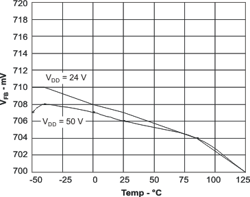
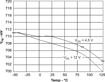
| VFB | Feedback voltage | COMP = FB, TA = 25°C | 689 | 696 | 702 | mV | |
| 4.5 < VDD < 52 | TA = 25°C | 686 | 696 | 703 | |||
| –40°C < TA < 85°C | 679 | 696 | 708 | ||||
| –40°C < TA < 125°C | 679 | 696 | 710 | ||||
| GATE DRIVER | |||||||
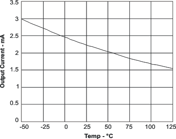
| Isrc | Gate driver pull-up current | 125 | 300 | mA | |||
| Isnk | Gate driver pull-down current | 200 | 300 | mA | |||
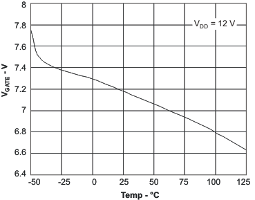
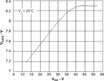
| VGATE | Gate driver output voltage | VGATE = (VDD – VGDRV), for 12 < VDD < 52 | 6 | 8 | 10 | V | |
| QUIESCENT CURRENT | |||||||
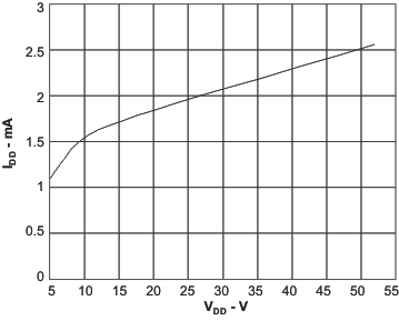
| Iqq | Device quiescent current | fOSC = 300 kHz, Driver not switching, 4.5 < VDD < 52 | 1.5 | 3.0 | mA | ||
| UNDERVOLTAGE LOCKOUT (UVLO) | |||||||
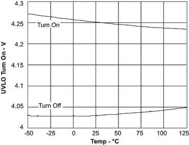
| VUVLO(on) | Turn-on threshold | –40°C < TA < 125°C | 3.8 | 4.25 | 4.5 | V | |
| VUVLO(off) | Turn-off threshold | 4.05 | |||||
| VUVLO(HYST) | Hysteresis | 110 | 200 | 275 | mV | ||
| SOFT-START | |||||||
| RSS(chg) | Internal soft-start pull-up resistance | 65 | 105 | 170 | kΩ | ||
| RSS(dchg) | Internal soft-start pull-down resistance | 190 | 305 | 485 | |||
| VSSRST | Soft-start reset threshold | 100 | 150 | 200 | mV | ||
| OVERCURRENT PROTECTION | |||||||
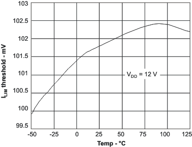
| VILIM | Overcurrent threshold | 4.5 < VDD < 52 | 0°C < TA < 125°C | 65 | 100 | 140 | mV |
| –40°C < TA < 125°C | 55 | 100 | 140 | ||||
| OCDF | Overcurrent duty cycle(1) | 2% | |||||
| VILIM(rst) | Overcurrent reset threshold | 100 | 150 | 200 | mV | ||
| OSCILLATOR | |||||||
| fOSC | Oscillator frequency range(1) | 35 | 500 | kHz | |||
| Oscillator frequency | RRC = 200 kΩ, CRC = 470 pF | 85 | 100 | 115 | |||
| RRC = 68.1 kΩ, CRC = 470 pF | 255 | 300 | 345 | ||||
| Frequency line regulation | 12 V < VDD < 52 V | -9% | 0% | ||||
| 4.5 V < VDD < 12 V | –20% | 0% | |||||
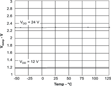
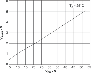
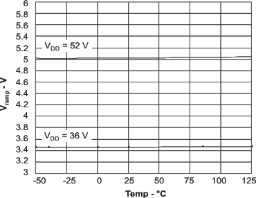
| VRMP | Ramp amplitude | 4.5 V < VDD < 52 V | VDD÷10 | V | |||
| PULSE WIDTH MODULATOR | |||||||
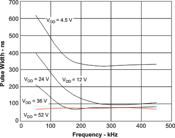
| tMIN | Minimum controllable pulse width(2) | VDD = 12 V | 200 | 400 | ns | ||
| VDD = 30 V | 100 | 200 | |||||
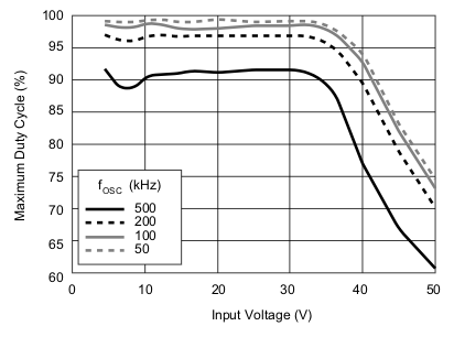
| DMAX | Maximum duty cycle | fosc = 100 kHz, CL = 470 pF | 93% | 95% | |||
| fosc = 300 kHz, CL = 470 pF | 90% | 93% | |||||
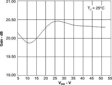
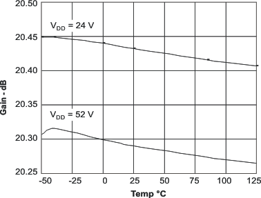
| KPWM | Modulator and power stage DC gain | 8 | 10 | 12 | V/V | ||
| ERROR AMPLIFIER | |||||||
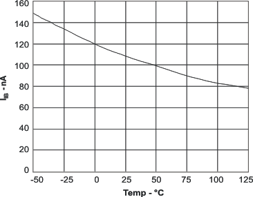
| IIB | Input bias current | 100 | 250 | nA | |||
| AOL | Open loop gain(1) | 60 | 80 | dB | |||
| GBWP | Unity gain bandwidth(1) | 1.5 | 3 | MHz | |||
| ICOMP(src) | Output source current | VFB = 0.6 V, COMP = 1 V | 100 | 250 | μA | ||
| ICOMP(snk) | Output sink current | VFB = 1.2 V, COMP = 1 V | 1.0 | 2.5 | mA | ||
(1) Ensured by design. Not production tested.
(2) See Figure 21 for for tMIN vs fOSC at various input voltages.
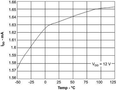
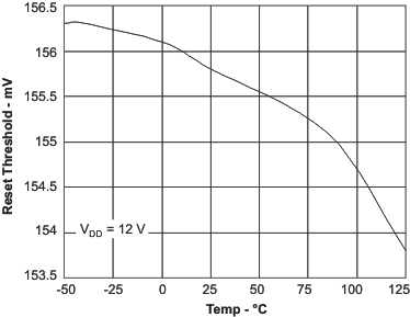
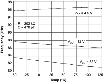
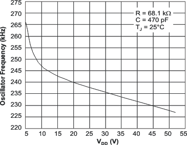
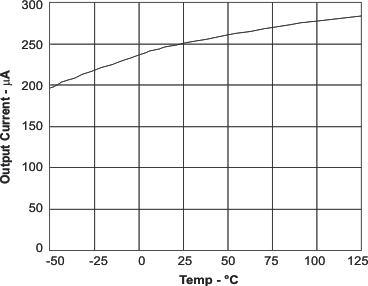
6.6 Typical Characteristics