SLVSD45 December 2015 TPS50601-SP
PRODUCTION DATA.
- 1 Features
- 2 Applications
- 3 Description
- 4 Revision History
- 5 Description (continued)
- 6 Pin Configuration and Functions
- 7 Specifications
-
8 Detailed Description
- 8.1 Overview
- 8.2 Functional Block Diagram
- 8.3
Feature Description
- 8.3.1 VIN and Power VIN Pins (VIN and PVIN)
- 8.3.2 PVIN vs Frequency
- 8.3.3 Voltage Reference
- 8.3.4 Adjusting the Output Voltage
- 8.3.5 Maximum Duty Cycle Limit
- 8.3.6 PVIN vs Frequency
- 8.3.7 Safe Start-Up into Prebiased Outputs
- 8.3.8 Error Amplifier
- 8.3.9 Slope Compensation
- 8.3.10 Enable and Adjust UVLO
- 8.3.11 Adjustable Switching Frequency and Synchronization (SYNC)
- 8.3.12 Slow Start (SS/TR)
- 8.3.13 Power Good (PWRGD)
- 8.3.14 Bootstrap Voltage (BOOT) and Low Dropout Operation
- 8.3.15 Sequencing (SS/TR)
- 8.3.16 Output Overvoltage Protection (OVP)
- 8.3.17 Overcurrent Protection
- 8.3.18 TPS50601-SP Thermal Shutdown
- 8.3.19 Turn-On Behavior
- 8.3.20 Small Signal Model for Loop Response
- 8.3.21 Simple Small Signal Model for Peak Current Mode Control
- 8.3.22 Small Signal Model for Frequency Compensation
- 8.4 Device Functional Modes
-
9 Application and Implementation
- 9.1 Application Information
- 9.2
Typical Application
- 9.2.1 Design Requirements
- 9.2.2
Detailed Design Procedure
- 9.2.2.1 Operating Frequency
- 9.2.2.2 Output Inductor Selection
- 9.2.2.3 Output Capacitor Selection
- 9.2.2.4 Input Capacitor Selection
- 9.2.2.5 Slow Start Capacitor Selection
- 9.2.2.6 Bootstrap Capacitor Selection
- 9.2.2.7 Undervoltage Lockout (UVLO) Set Point
- 9.2.2.8 Output Voltage Feedback Resistor Selection
- 9.2.2.9 Compensation Component Selection
- 9.2.3 Application Curve
- 10Power Supply Recommendations
- 11Layout
- 12Device and Documentation Support
- 13Mechanical, Packaging, and Orderable Information
Package Options
Mechanical Data (Package|Pins)
- HKH|20
- KGD|0
Thermal pad, mechanical data (Package|Pins)
Orderable Information
1 Features
-
5962R10221:
- Radiation Hardness Assurance (RHA) up to TID 100 krad (Si)
- ELDRS Free 100 krad (Si) – 10 mRAD(Si)/s
- Single Event Latchup (SEL) Immune to
LET = 85 MeV-cm2/mg (See Radiation Report) - SEB and SEGR Immune to 85 MeV-cm2/mg, SOA Curve Available (See Radiation Report)
- SET/SEFI Cross-Section Plot Available (See Radiation Report)
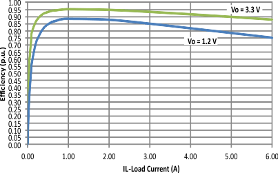
- Peak Efficiency: 95% (VO = 3.3 V)
- Integrated 55-mΩ/50-mΩ MOSFETs
- Split Power Rail: 1.6 to 6.3 V on PVIN
- Power Rail: 3 to 6.3 V on VIN
- 6-A Maximum Output Current
- Flexible Switching Frequency Options:
- 100-kHz to 1-MHz Adjustable Internal Oscillator
- External Sync Capability: 100 kHz to 1 MHz
- Sync Pin can be Configured as a 500-kHz Output for Master/Slave Applications
- 0.795-V ±1.258% Voltage Reference at 25°C
- Monotonic Start-Up into Prebiased Outputs
- Adjustable Soft Start Through External Capacitor
- Input Enable and Power-Good Output for Power Sequencing
- Power Good Output Monitor for Undervoltage and Overvoltage
- Adjustable Input Undervoltage Lockout (UVLO)
- 20-Pin Thermally-Enhanced Ceramic Flatpack Package (HKH)
- See www.ti.com/swift for SWIFT™ Documentation
- See the Tools & Software Tab
Efficiency vs Load Current, Vin = 5 V

2 Applications
- Space Satellite Point of Load Supply for FPGAs, Microcontrollers, and ASICs
- Space Satellite Payloads
- Radiation-Tolerant Applications
- Available in Military (–55°C to 125°C) Temperature Range
- Engineering Evaluation (/EM) Samples are Available(1)
3 Description
The TPS50601-SP is a radiation hardened, 6.3-V, 6-A synchronous step-down converter, which is optimized for small designs through high efficiency and integrating the high-side and low-side MOSFETs. Further space savings are achieved through current mode control, which reduces component count, and a high switching frequency, reducing the inductor's footprint. The devices are offered in a thermally enhanced 20-pin ceramic, dual in-line flatpack package.
Device Information(2)
| PART NUMBER | PACKAGE | BODY SIZE (NOM) |
|---|---|---|
| TPS50601-SP | CFP (20) | 7.38 × 12.70 mm |
| KGD(3) | N/A(4) |
- These units are intended for engineering evaluation only. They are processed to a non-compliant flow (that is no burn-in, and so forth) and are tested to temperature rating of 25°C only. These units are not suitable for qualification, production, radiation testing or flight use. Parts are not warranted for performance on full MIL specified temperature range of –55°C to 125°C or operating life.
- For all available packages, see the orderable addendum at the end of the data sheet.
- Known good die
- Bare die in waffle pack
SPACE
SPACE
4 Revision History
| DATE | REVISION | NOTES |
|---|---|---|
| December 2015 | * |
Initial release. |