SLUSCA7A November 2015 – July 2022 TPS51216-EP
PRODUCTION DATA
- 1 Features
- 2 Applications
- 3 Description
- 4 Revision History
- 5 Description (continued)
- 6 Pin Configuration and Functions
- 7 Specifications
- 8 Detailed Description
- 9 Application and Implementation
- 10Power Supply Recommendations
- 11Layout
- 12Device and Documentation Support
- 13Mechanical, Packaging, and Orderable Information
Package Options
Mechanical Data (Package|Pins)
- RUK|20
Thermal pad, mechanical data (Package|Pins)
- RUK|20
Orderable Information
9.2.2.2 External Components Selection
The external components selection is simple in D-CAP mode.
- Determine the value of R4 and R5.
The output voltage is determined by the value of the voltage-divider resistor, R4 and R5, as shown in Figure 9-4. R4 is connected between VREF and REFIN pins, and R5 is connected between the REFIN pin and GND. Setting R4 as 10-kΩ is a good starting point. Determine R5 using Equation 7.
Equation 7.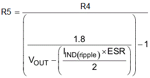
- Choose the inductor.
The inductance value should be determined to yield a ripple current of approximately ¼ to ½ of maximum output current. Larger ripple current increases output ripple voltage and improves the signal-to-noise ratio and helps stable operation.
Equation 8.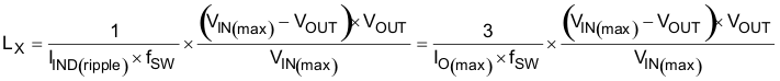
The inductor needs a low direct current resistance (DCR) to achieve good efficiency, as well as enough room above peak inductor current before saturation. The peak inductor current can be estimated in Equation 9.
Equation 9.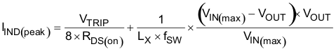
- Choose the OCL setting resistance,
RTRIP.
Combining Equation 4 and Equation 5, RTRIP can be obtained using Equation 10.
Equation 10.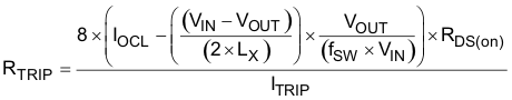
- Choose the output capacitors.
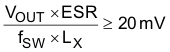
TI recommends organic semiconductor capacitors or specialty polymer capacitors. Determine ESR to meet small signal stability and recommended ripple voltage. A quick reference is shown in Equation 11 and Equation 12.
Equation 11.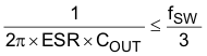 Equation 12.