SLVSEY3C February   2019  – April 2021 TPS51396A

PRODUCTION DATA  

  1. Features
  2. Applications
  3. Description
  4. Revision History
  5. Pin Configuration and Functions
  6. Specifications
    1. 6.1 Absolute Maximum Ratings
    2. 6.2 ESD Ratings
    3. 6.3 Recommended Operating Conditions
    4. 6.4 Thermal Information
    5. 6.5 Electrical Characteristics
    6. 6.6 Typical Characteristics
  7. Detailed Description
    1. 7.1 Overview
    2. 7.2 Functional Block Diagram
    3. 7.3 Feature Description
      1. 7.3.1 PWM Operation and D-CAP3 Control
      2. 7.3.2 Soft Start
      3. 7.3.3 Large Duty Operation
      4. 7.3.4 Power Good
      5. 7.3.5 Over Current Protection and Undervoltage Protection
      6. 7.3.6 Over Voltage Protection
      7. 7.3.7 UVLO Protection
      8. 7.3.8 Output Voltage Discharge
      9. 7.3.9 Thermal Shutdown
    4. 7.4 Device Functional Modes
      1. 7.4.1 Light Load Operation
      2. 7.4.2 Advanced Eco-mode Control
      3. 7.4.3 Out of Audio Mode
      4. 7.4.4 Mode Selection
      5. 7.4.5 Standby Operation
  8. Application and Implementation
    1. 8.1 Application Information
    2. 8.2 1V Output Typical Application
      1. 8.2.1 Design Requirements
      2. 8.2.2 Detailed Design Procedure
        1. 8.2.2.1 External Component Selection
          1. 8.2.2.1.1 Output Voltage Set Point
          2. 8.2.2.1.2 Inductor Selection
          3. 8.2.2.1.3 Output Capacitor Selection
          4. 8.2.2.1.4 Input Capacitor Selection
      3. 8.2.3 Application Curves
  9. Power Supply Recommendations
  10. 10Layout
    1. 10.1 Layout Guidelines
    2. 10.2 Layout Example
  11. 11Device and Documentation Support
    1. 11.1 Device Support
      1. 11.1.1 Third-Party Products Disclaimer
    2. 11.2 Receiving Notification of Documentation Updates
    3. 11.3 Support Resources
    4. 11.4 Trademarks
    5. 11.5 Electrostatic Discharge Caution
    6. 11.6 Glossary
  12. 12Mechanical, Packaging, and Orderable Information

Package Options

Refer to the PDF data sheet for device specific package drawings

Mechanical Data (Package|Pins)
  • RJE|20
Thermal pad, mechanical data (Package|Pins)
Orderable Information
Input Capacitor Selection

The TPS51396A requires input decoupling capacitors on power supply input VIN, and the bulk capacitors are needed depending on the application. The minimum input capacitance required is given in Equation 7.

Equation 7. GUID-71780B95-389B-45E5-B6CF-C936490D3D49-low.gif

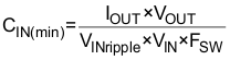
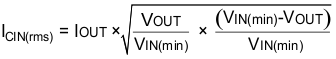
TI recommends using a high-quality X5R or X7R input decoupling capacitors of 40 µF on the input voltage pin VIN. The voltage rating on the input capacitor must be greater than the maximum input voltage. The capacitor must also have a ripple current rating greater than the maximum input current ripple of the application. The input ripple current is calculated by Equation 8:

Equation 8. GUID-7499CF2A-DAB9-43B5-B11F-B7B5DF13BBAA-low.gif

A 1-µF ceramic capacitor is needed for the decoupling capacitor on VCC pin.