SLVSEY3C February 2019 – April 2021 TPS51396A
PRODUCTION DATA
- 1 Features
- 2 Applications
- 3 Description
- 4 Revision History
- 5 Pin Configuration and Functions
- 6 Specifications
- 7 Detailed Description
- 8 Application and Implementation
- 9 Power Supply Recommendations
- 10Layout
- 11Device and Documentation Support
- 12Mechanical, Packaging, and Orderable Information
Package Options
Refer to the PDF data sheet for device specific package drawings
Mechanical Data (Package|Pins)
- RJE|20
Thermal pad, mechanical data (Package|Pins)
- RJE|20
Orderable Information
3 Description
The TPS51396A is a cost-effective, high-voltage input, high-efficiency synchronous buck converter with integrated FETs.
The key feature of the TPS51396A is its ULQ (Ultra Low Quiescent) feature to enable low-bias current and large duty operation. The ULQ feature is extremely beneficial for long battery life in low power operation. The TPS51396A operates with a supply input voltage ranging from 4.5 V to 24 V. It uses DCAP3 control mode to provide a fast transient response, good line, load regulation, no requirement for external compensation, and supports low equivalent series resistance (ESR) output capacitors such as specialty polymer and ultra-low ESR ceramic capacitors.
The TPS51396A provides complete protection OVP, UVP, OCP, OTP, and UVLO. It is combined power good signal and output discharge function.
The MODE pin in the TPS51396A can be used to set Eco-Mode or OOA mode for light load operation. The Eco-Mode maintains high efficiency during light load operation, and OOA mode operations with switching frequency larger than 25 kHz even no loading.
The TPS51396A supports both an internal and external soft-start time option. It has the internal fixed soft-start time of 1.3 ms. If the application needs longer soft-start time, the external SS pin can be used to achieve it by connecting the external capacitor.
The TPS51396A is available in a 20-pin 3.0-mm × 3.0-mm HotRod package and the junction temperature is specified from –40°C to 125°C.
| PART NUMBER | PACKAGE(1) | BODY SIZE (NOM) |
|---|---|---|
| TPS51396A | VQFN (20) | 3.00 mm × 3.00 mm |
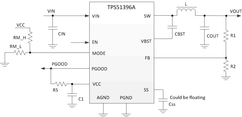
 Typical Application
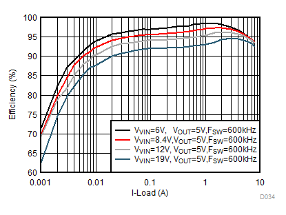
 Efficiency vs Output Current
ECO-mode