SLUSAE1F December 2010 – December 2018 TPS51916
PRODUCTION DATA.
- 1 Features
- 2 Applications
- 3 Description
- 4 Revision History
- 5 Pin Configuration and Functions
- 6 Specifications
-
7 Detailed Description
- 7.1 Overview
- 7.2 Functional Block Diagram
- 7.3
Feature Description
- 7.3.1 VDDQ Switch Mode Power Supply Control
- 7.3.2 VREF and REFIN, VDDQ Output Voltage
- 7.3.3 Soft-Start and Powergood
- 7.3.4 Power State Control
- 7.3.5 Discharge Control
- 7.3.6 VTT and VTTREF
- 7.3.7 VDDQ Overvoltage and Undervoltage Protection
- 7.3.8 VDDQ Out-of-Bound Operation
- 7.3.9 VDDQ Overcurrent Protection
- 7.3.10 VTT Overcurrent Protection
- 7.3.11 V5IN Undervoltage Lockout Protection
- 7.3.12 Thermal Shutdown
- 7.4 Device Functional Modes
- 7.5 D-CAP2™ Mode Operation
- 8 Application and Implementation
- 9 Power Supply Recommendations
- 10Layout
- 11Device and Documentation Support
- 12Mechanical, Packaging, and Orderable Information
Package Options
Mechanical Data (Package|Pins)
- RUK|20
Thermal pad, mechanical data (Package|Pins)
- RUK|20
Orderable Information
7.4.2 D-CAP™ Mode
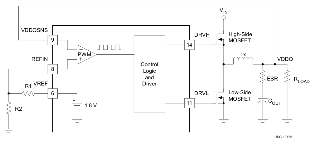
Figure 36 shows a simplified model of D-CAP™ mode architecture.
 Figure 36. Simplified D-CAP™ Model
 The VDDQSNS voltage is compared with REFIN voltage. The PWM comparator creates a set signal to turn on the high-side MOSFET. The gain and speed of the comparator is high enough to maintain the voltage at the beginning of each on-cycle (or the end of each off-cycle) to be substantially constant. The DC output voltage monitored at VDDQ may have line regulation due to ripple amplitude that slightly increases as the input voltage increase. The D-CAP™ mode offers flexibility on output inductance and capacitance selections with ease-of-use without complex feedback loop calculation and external components. However, it does require a sufficient level of ESR that represents inductor current information for stable operation and good jitter performance. Organic semiconductor capacitor(s) or specialty polymer capacitor(s) are recommended.
The requirement for loop stability is simple and is described in Equation 3. The 0-dB frequency, f0 defined in Equation 3, is recommended to be lower than 1/3 of the switching frequency to secure proper phase margin.

where
- ESR is the effective series resistance of the output capacitor
- COUT is the capacitance of the output capacitor
- fsw is switching frequency
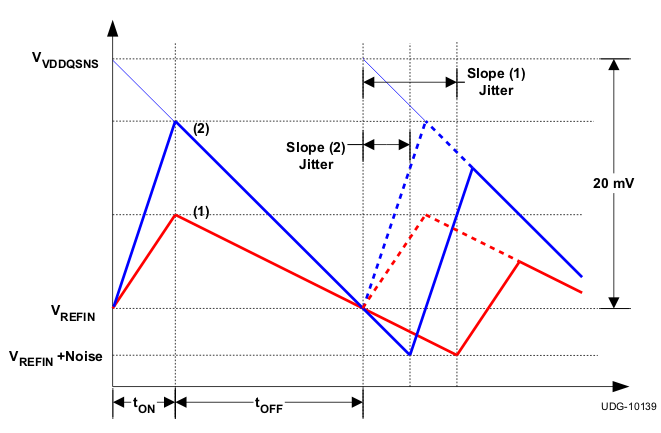
Jitter is another attribute caused by signal-to-noise ratio of the feedback signal. One of the major factors that determine jitter performance in D-CAP™ mode is the down-slope angle of the VDDQSNS ripple voltage. Figure 37 shows, in the same noise condition, that jitter is improved by making the slope angle larger.
 Figure 37. Ripple Voltage Slope and Jitter Performance
 For a good jitter performance, use the recommended down slope of approximately 20 mV per switching period as shown in Figure 37 and Equation 4.

where
- VOUT is the VDDQ output voltage
- LX is the inductance