SLUSAE1F December 2010 – December 2018 TPS51916
PRODUCTION DATA.
- 1 Features
- 2 Applications
- 3 Description
- 4 Revision History
- 5 Pin Configuration and Functions
- 6 Specifications
-
7 Detailed Description
- 7.1 Overview
- 7.2 Functional Block Diagram
- 7.3
Feature Description
- 7.3.1 VDDQ Switch Mode Power Supply Control
- 7.3.2 VREF and REFIN, VDDQ Output Voltage
- 7.3.3 Soft-Start and Powergood
- 7.3.4 Power State Control
- 7.3.5 Discharge Control
- 7.3.6 VTT and VTTREF
- 7.3.7 VDDQ Overvoltage and Undervoltage Protection
- 7.3.8 VDDQ Out-of-Bound Operation
- 7.3.9 VDDQ Overcurrent Protection
- 7.3.10 VTT Overcurrent Protection
- 7.3.11 V5IN Undervoltage Lockout Protection
- 7.3.12 Thermal Shutdown
- 7.4 Device Functional Modes
- 7.5 D-CAP2™ Mode Operation
- 8 Application and Implementation
- 9 Power Supply Recommendations
- 10Layout
- 11Device and Documentation Support
- 12Mechanical, Packaging, and Orderable Information
Package Options
Mechanical Data (Package|Pins)
- RUK|20
Thermal pad, mechanical data (Package|Pins)
- RUK|20
Orderable Information
3 Description
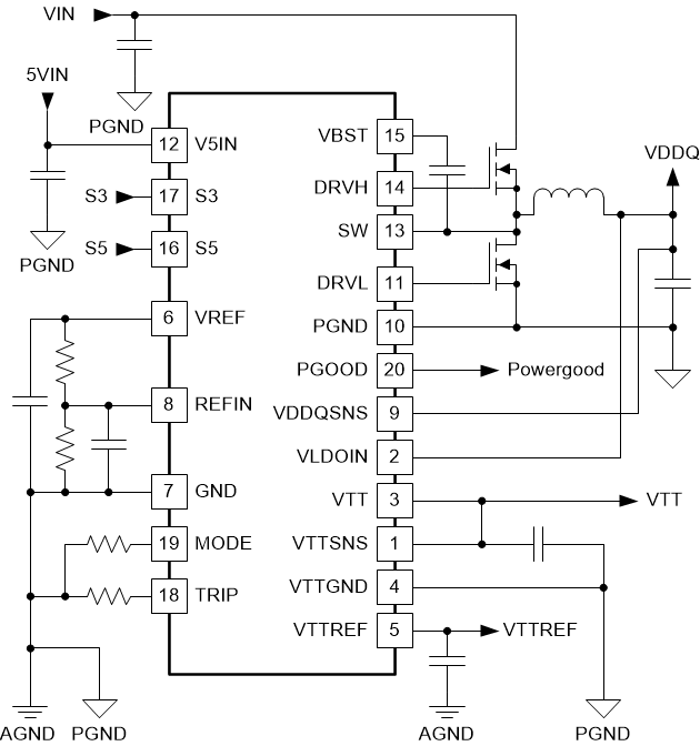
The TPS51916 device provides a complete power supply for DDR2, DDR3, DDR3L, and DDR4 memory systems in the lowest total cost and minimum space. It integrates a synchronous buck regulator controller (VDDQ) with a 2-A sink and 2-A source tracking LDO (VTT) and buffered low noise reference (VTTREF).
The device employs D-CAP™ mode coupled with 300 kHz or 400 kHz frequencies for ease-of-use and fast transient response or D-CAP2™ mode coupled with higher 500 kHz or 670 kHz frequencies to support ceramic output capacitor without an external compensation circuit. The VTTREF tracks VDDQ/2 within excellent 0.8% accuracy. The VTT, which provides 2-A sink and 2-A source peak current capabilities, requires only 10-μF of ceramic capacitance. A dedicated LDO supply input is available.
The device also provides excellent power supply performance. It supports flexible power state control, placing VTT at high-Z in S3 and discharging VDDQ, VTT and VTTREF (soft-off) in S4 or S5 state. Programmable OCL with low-side MOSFET RDS(on) sensing, OVP, UVP, UVLO and thermal shutdown protections are also available.
Device Information(1)
| PART NUMBER | PACKAGE | BODY SIZE (NOM) |
|---|---|---|
| TPS51916 | QFN (20) | 3 mm × 3 mm |
- For all available packages, see the orderable addendum at the end of the data sheet.
Simplified Application

.