SLUSAE1F December 2010 – December 2018 TPS51916
PRODUCTION DATA.
- 1 Features
- 2 Applications
- 3 Description
- 4 Revision History
- 5 Pin Configuration and Functions
- 6 Specifications
-
7 Detailed Description
- 7.1 Overview
- 7.2 Functional Block Diagram
- 7.3
Feature Description
- 7.3.1 VDDQ Switch Mode Power Supply Control
- 7.3.2 VREF and REFIN, VDDQ Output Voltage
- 7.3.3 Soft-Start and Powergood
- 7.3.4 Power State Control
- 7.3.5 Discharge Control
- 7.3.6 VTT and VTTREF
- 7.3.7 VDDQ Overvoltage and Undervoltage Protection
- 7.3.8 VDDQ Out-of-Bound Operation
- 7.3.9 VDDQ Overcurrent Protection
- 7.3.10 VTT Overcurrent Protection
- 7.3.11 V5IN Undervoltage Lockout Protection
- 7.3.12 Thermal Shutdown
- 7.4 Device Functional Modes
- 7.5 D-CAP2™ Mode Operation
- 8 Application and Implementation
- 9 Power Supply Recommendations
- 10Layout
- 11Device and Documentation Support
- 12Mechanical, Packaging, and Orderable Information
Package Options
Mechanical Data (Package|Pins)
- RUK|20
Thermal pad, mechanical data (Package|Pins)
- RUK|20
Orderable Information
7.3.6 VTT and VTTREF
The TPS51916 device integrates two high-performance, low-drop-out linear regulators, VTT and VTTREF, to provide complete DDR2, DDR3, DDR3L, and DDR4 power solutions. The VTTREF has a 10-mA sink/source current capability, and tracks ½ of VDDQSNS with ±1% accuracy using an on-chip ½ divider. A 0.22-μF (or larger) ceramic capacitor must be connected close to the VTTREF terminal to ensure stable operation. The VTT responds quickly to track VTTREF within ±40 mV at all conditions, and the current capability is 2 A for both sink and source. A 10-μF (or larger) ceramic capacitor(s) need to be connected close to the VTT terminal for stable operation. To achieve tight regulation with minimum effect of wiring resistance, a remote sensing terminal, VTTSNS, should be connected to the positive node of VTT output capacitors as a separate trace from the high-current line to the VTT pin. (Refer to the Layout section for details.)
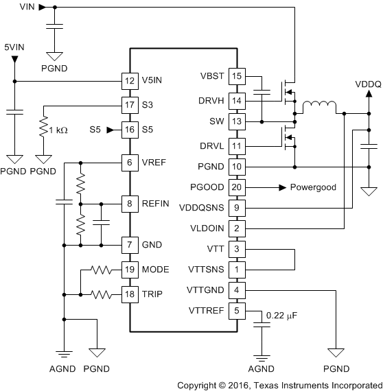
When VTT is not required in the design, following treatment is strongly recommended.
- Connect VLDOIN to VDDQ.
- Tie VTTSNS to VTT, and remove capacitors from VTT to float.
- Connect VTTGND to GND.
- Select MODE2, 3, 4 or 5 shown in Table 2 (Select Non-tracking discharge mode).
- Maintain a 0.22-µF capacitor connected at VTTREF.
- Pull down S3 to GND with 1-kΩ resistance.
 Figure 35. Application Circuit When VTT Is Not Required