SLUSAE1F December 2010 – December 2018 TPS51916
PRODUCTION DATA.
- 1 Features
- 2 Applications
- 3 Description
- 4 Revision History
- 5 Pin Configuration and Functions
- 6 Specifications
-
7 Detailed Description
- 7.1 Overview
- 7.2 Functional Block Diagram
- 7.3
Feature Description
- 7.3.1 VDDQ Switch Mode Power Supply Control
- 7.3.2 VREF and REFIN, VDDQ Output Voltage
- 7.3.3 Soft-Start and Powergood
- 7.3.4 Power State Control
- 7.3.5 Discharge Control
- 7.3.6 VTT and VTTREF
- 7.3.7 VDDQ Overvoltage and Undervoltage Protection
- 7.3.8 VDDQ Out-of-Bound Operation
- 7.3.9 VDDQ Overcurrent Protection
- 7.3.10 VTT Overcurrent Protection
- 7.3.11 V5IN Undervoltage Lockout Protection
- 7.3.12 Thermal Shutdown
- 7.4 Device Functional Modes
- 7.5 D-CAP2™ Mode Operation
- 8 Application and Implementation
- 9 Power Supply Recommendations
- 10Layout
- 11Device and Documentation Support
- 12Mechanical, Packaging, and Orderable Information
Package Options
Mechanical Data (Package|Pins)
- RUK|20
Thermal pad, mechanical data (Package|Pins)
- RUK|20
Orderable Information
7.5 D-CAP2™ Mode Operation
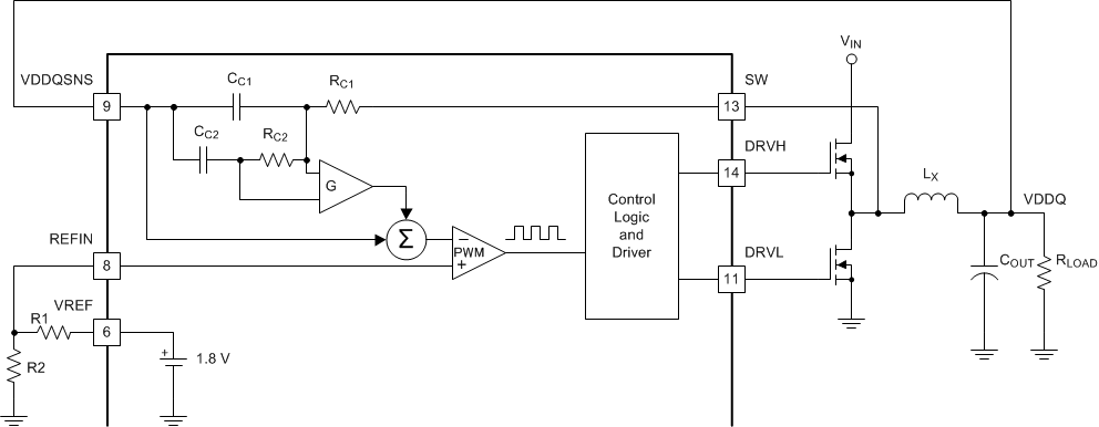
Figure 38 shows simplified model of D-CAP2™ architecture.
The D-CAP2™ mode in the TPS51916 device includes an internal feedback network enabling the use of very low ESR output capacitor(s) such as multi-layer ceramic capacitors. The role of the internal network is to sense the ripple component of the inductor current information and combine it with voltage feedback signal. Using RC1=RC2≡RC and CC1=CC2≡CC, 0-dB frequency of the D-CAP2™ mode is given by Equation 5. It is recommended that the 0-dB frequency (f0) be lower than 1/3 of the switching frequency to secure the proper phase margin

where
- G is gain of the amplifier which amplifies the ripple current information generated by the compensation circuit
The typical G value is 0.25, and typical RCCC time constant values for 500 kHz and 670 kHz operation are 23 µs and 14.6 µs, respectively.
For example, when fSW=500 kHz and LX=1 µH, COUT should be larger than 88 µF.
When selecting the capacitor, pay attention to its characteristics. For MLCC use X5R or better dielectric and consider the derating of the capacitance by both DC bias and AC bias. When derating by DC bias and AC bias are 80% and 50%, respectively, the effective derating is 40% because 0.8 x 0.5 = 0.4. The capacitance of specialty polymer capacitors may change depending on the operating frequency. Consult capacitor manufacturers for specific characteristics.
