SLUS825C February 2008 – August 2014 TPS53124
PRODUCTION DATA.
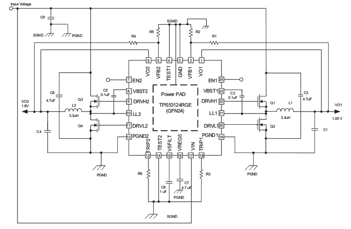
- 1Simplified Schematics
- 2Pin Configuration and Functions
- 3Specifications
- 4Detailed Description
-
5Application and Implementation
- 5.1 Application Information
- 5.2
Typical Application
- 5.2.1 Design Requirements
- 5.2.2
Detailed Design Procedure
- 5.2.2.1 Choose Inductor
- 5.2.2.2 Loop Compensation and External Parts Selection
- 5.2.2.3 Choose Input Capacitor
- 5.2.2.4 Choose Bootstrap Capacitor
- 5.2.2.5 Choose VREG5 and V5FILT Capacitor
- 5.2.2.6 Choose Output Voltage Set Point Resistors
- 5.2.2.7 Choose Over Current Set Point Resistor
- 5.2.2.8 Choose Soft Start Capacitor
- 5.2.3 Application Curves (QFN)
- 6Power Supply Recommendations
- 7Layout
Package Options
Mechanical Data (Package|Pins)
Thermal pad, mechanical data (Package|Pins)
- RGE|24
Orderable Information
Features
- High Efficiency, Low-Power Consumption
- D-Cap Mode Enables Fast Transient Response
- High Initial Reference Accuracy
- Low Output Ripple
- Wide Input Voltage Range: 4.5 V to 24 V
- Output Voltage Range: 0.76 V to 5.5 V
- Low-Side RDS(on) Loss-less Current Sensing
- Adaptive Gate Drivers with Integrated Boost Diode
- Internal 1.2-ms Voltage-Servo Soft Start
- Built-In 5-V Linear Regulator
Applications
- Digital TV Power Supply
- Networking Home Terminal
- Digital STB
Description
The TPS53124 is a dual, Adaptive on-time DCAP™ mode synchronous controller. The part enables system designers to cost effectively complete the suite of digital TV power bus regulators with the absolute lowest external component count and lowest standby consumption. The main control loop for the TPS53124 uses the D-CAP™ mode that optimized for low ESR output capacitors such as POSCAP or SP-CAP promises fast transient response with no external compensation. The part provides a convenient and efficient operation with conversion voltages from 4.5 V to 24 V and output voltage from 0.76 V to 5.5 V.
The TPS53124 is available in the 24-pin RGE package and in the 28-pin PW package and is specified from -40°C to 85°C ambient temperature range.
Device Information(1)
| DEVICE NAME | PACKAGE | BODY SIZE |
|---|---|---|
| TPS53124 | PW (28) | 9.70 mm x 6.40 mm |
| TPS53124 | QFN (24) | 4.00 mm x 4.00 mm |
- For all available packages, see the orderable addendum at the end of the datasheet.
1 Simplified Schematics