SLUS825C February 2008 – August 2014 TPS53124
PRODUCTION DATA.
- 1Simplified Schematics
- 2Pin Configuration and Functions
- 3Specifications
- 4Detailed Description
-
5Application and Implementation
- 5.1 Application Information
- 5.2
Typical Application
- 5.2.1 Design Requirements
- 5.2.2
Detailed Design Procedure
- 5.2.2.1 Choose Inductor
- 5.2.2.2 Loop Compensation and External Parts Selection
- 5.2.2.3 Choose Input Capacitor
- 5.2.2.4 Choose Bootstrap Capacitor
- 5.2.2.5 Choose VREG5 and V5FILT Capacitor
- 5.2.2.6 Choose Output Voltage Set Point Resistors
- 5.2.2.7 Choose Over Current Set Point Resistor
- 5.2.2.8 Choose Soft Start Capacitor
- 5.2.3 Application Curves (QFN)
- 6Power Supply Recommendations
- 7Layout
Package Options
Mechanical Data (Package|Pins)
Thermal pad, mechanical data (Package|Pins)
- RGE|24
Orderable Information
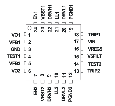
2 Pin Configuration and Functions
QFN Package
24 Pins
Top View
TSSOP Package
28 Pins
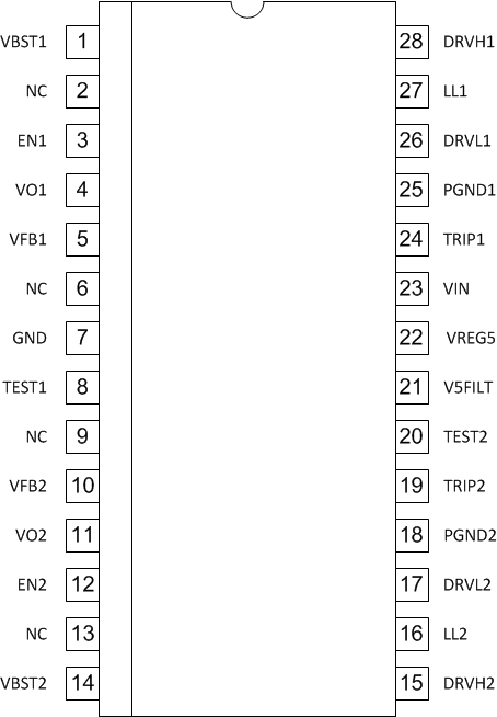
Pin Functions
| PIN | I/O | DESCRIPTION | ||
|---|---|---|---|---|
| NAME | GFN24 | TSSOP28 | ||
| VBST1, VBST2 | 23, 8 | 1, 14 | I | Supply input for high-side NFET driver (boost terminal). Connect capacitor from this pin to respective LL terminals. An internal PN diode is connected between VREG5 to each of these pins. User can add external schottky diode if forward drop is critical to drive the NFET. |
| EN1, EN2 | 24, 7 | 3, 12 | I | Channel 1 and Channel 2 enable pins. |
| VO1, VO2 | 1, 6 | 4, 11 | I | Output connections to SMPS. These terminals serve ON-time adjustment, output discharge. |
| VFB1, VFB2 | 2, 5 | 5, 10 | I | SMPS feedback inputs. Connect with feedback resistor divider. |
| GND | 3 | 7 | I | Signal ground pin. |
| DRVH1, DRVH2 | 22, 9 | 28, 15 | O | High-side NFET driver outputs. LL referenced floating drivers. The gate drive voltage is defined by the voltage across VBST to LL node flying capacitor. |
| LL1, LL2 | 21, 10 | 27, 16 | I/O | Switch-node connections for high-side drivers. Also serve as input to current comparators. |
| DRVL1, DRVL2 | 20, 11 | 26, 17 | O | Synchronous NFET driver outputs. PGND referenced drivers. The gate drive voltage is defined by VREG5 voltage. |
| PGND1, PGND2 | 19, 12 | 25, 18 | I/O | Ground returns for DRVL1 and DRVL2. Also serve as input of current comparators. Connect PGND1, PGND2 and GND strongly together near the device. |
| TRIP1, TRIP2 | 18, 13 | 24, 19 | I | Over-current trip point set input. Connect resistor from this pin to GND to set threshold for synchronous RDS(on) sense. Voltage across this pin and GND is compared to voltage across PGND and LL at over current comparator. |
| VIN | 17 | 23 | I | Supply Input for 5-V linear regulator. |
| V5FILT | 15 | 21 | I | 5-V supply input for the entire control circuit except the NFET drivers. Connect capacitor (typical 1 μF) from GND to V5FILT. V5FILT is connected to VREG5 via internal resistor. |
| VREG5 | 16 | 20 | O | 5-V power supply output. VREG5 is connected to V5FILT via internal resistor. |
| TEST1, TEST2 | 4, 14 | 8, 20 | I/O | Used for test only. Pin should be connected to GND |