SLUS825C February 2008 – August 2014 TPS53124
PRODUCTION DATA.
- 1Simplified Schematics
- 2Pin Configuration and Functions
- 3Specifications
- 4Detailed Description
-
5Application and Implementation
- 5.1 Application Information
- 5.2
Typical Application
- 5.2.1 Design Requirements
- 5.2.2
Detailed Design Procedure
- 5.2.2.1 Choose Inductor
- 5.2.2.2 Loop Compensation and External Parts Selection
- 5.2.2.3 Choose Input Capacitor
- 5.2.2.4 Choose Bootstrap Capacitor
- 5.2.2.5 Choose VREG5 and V5FILT Capacitor
- 5.2.2.6 Choose Output Voltage Set Point Resistors
- 5.2.2.7 Choose Over Current Set Point Resistor
- 5.2.2.8 Choose Soft Start Capacitor
- 5.2.3 Application Curves (QFN)
- 6Power Supply Recommendations
- 7Layout
Package Options
Mechanical Data (Package|Pins)
Thermal pad, mechanical data (Package|Pins)
- RGE|24
Orderable Information
7 Layout
7.1 Layout Guidelines
- Keep the input switching current loop as small as possible. (VIN ≥ C3 ≥ PNGD ≥ Sync FET ≥ SW ≥ Control FET)
- Place the input capacitor (C3) close to the top switching FET. The output current loop should also be kept as small as possible.
- Keep the SW node as physically small and short as possible as to minimize parasitic capacitance and inductance and to minimize radiated emissions. Kelvin connections should be brought from the output to the feedback terminal (FBx) of the device.
- Keep analog and non-switching components away from switching components.
- Make a single point connection from the signal ground to power ground.
- Do not allow switching current to flow under the device.
- DRVH and DRVL line should not run close to SW node or minimize it.
- GND terminals for capacitors of SSx and V5FILT and resistors of feedback and TRIPx should be connected to SGND.
- GND terminals for capacitors of VREG5 and VIN should be connected to PGND.
- Signal lines should not run under/near output inductor or minimize it.
7.2 Layout Example
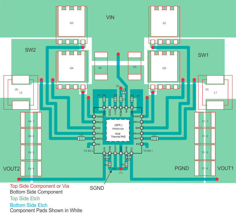 Figure 15. Layout Example for QFN