SLUS825C February 2008 – August 2014 TPS53124
PRODUCTION DATA.
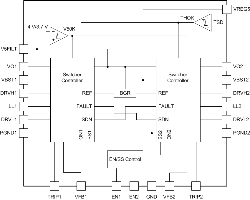
- 1Simplified Schematics
- 2Pin Configuration and Functions
- 3Specifications
- 4Detailed Description
-
5Application and Implementation
- 5.1 Application Information
- 5.2
Typical Application
- 5.2.1 Design Requirements
- 5.2.2
Detailed Design Procedure
- 5.2.2.1 Choose Inductor
- 5.2.2.2 Loop Compensation and External Parts Selection
- 5.2.2.3 Choose Input Capacitor
- 5.2.2.4 Choose Bootstrap Capacitor
- 5.2.2.5 Choose VREG5 and V5FILT Capacitor
- 5.2.2.6 Choose Output Voltage Set Point Resistors
- 5.2.2.7 Choose Over Current Set Point Resistor
- 5.2.2.8 Choose Soft Start Capacitor
- 5.2.3 Application Curves (QFN)
- 6Power Supply Recommendations
- 7Layout
Package Options
Mechanical Data (Package|Pins)
Thermal pad, mechanical data (Package|Pins)
- RGE|24
Orderable Information
4 Detailed Description
4.1 Overview
The TPS53124 is a dual, Adaptive on-time DCAP™ mode synchronous controller. The part enables system designers to cost effectively complete the suite of digital TV power bus regulators with the absolute lowest external component count and lowest standby consumption. The main control loop for the TPS53124 uses the D-CAP™ mode that optimized for low ESR output capacitors such as POSCAP or SP-CAP promises fast transient response with no external compensation. The part provides a convenient and efficient operation with conversion voltages from 4.5 V to 24 V and output voltage from 0.76 V to 5.5 V.
4.2 Functional Block Diagram
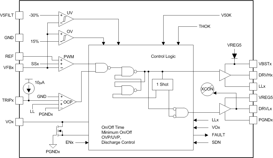
4.3 Feature Description
4.3.1 PWM Operation
The main control loop of the switching mode power supply (SMPS) is designed as an adaptive on-time pulse width modulation (PWM) controller. It supports a proprietary D-CAP™ Mode. D-CAP™ Mode uses internal compensation circuit and is suitable for low external component count configuration with appropriate amount of ESR at the output capacitor(s). The output ripple bottom voltage is monitored at a feedback point voltage.
At the beginning of each cycle, the synchronous high-side MOSFET is turned on, or becomes ON state. This MOSFET is turned off, or becomes OFF state, after internal one-shot timer expires. This one shot is determined by the converter’s input voltage ,VIN, and the output voltage ,VOUT, to keep frequency fairly constant over the input voltage range, hence it is called adaptive on-time control. The high-side MOSFET is turned on again when feedback information indicates insufficient output voltage. Repeating operation in this manner, the controller regulates the output voltage.
4.3.2 Low-Side Driver
The low-side driver is designed to drive high current low RDS(on) N-channel MOSFET(s). The drive capability is represented by its internal resistance. A dead time to prevent shoot through is internally generated between high-side MOSFET off to low-side MOSFET on, and low-side MOSFET off to high-side MOSFET on. 5-V bias voltage is delivered from internal regulator VREG5 output. The instantaneous drive current is supplied by an input capacitor connected between VREG5 and GND. The average drive current is equal to the gate charge at VGS = 5 V times switching frequency. This gate drive current as well as the high-side gate drive current times 5 V makes the driving power which need to be dissipated from TPS53124 package.
4.3.3 High-Side Driver
The high-side driver is designed to drive high current, low RDS(on) N-channel MOSFET(s). When configured as a floating driver, 5-V bias voltage is delivered from VREG5 supply. The average drive current is also calculated by the gate charge at VGS = 5 V times switching frequency. The instantaneous drive current is supplied by the flying capacitor between VBSTx and LLx pins. The drive capability is represented by its internal resistance.
4.3.4 PWM Frequency and Adaptive On-Time Control
TPS53124 employs adaptive on-time control scheme and does not have a dedicated oscillator on board. However, the part runs with pseudo-constant frequency by feed-forwarding the input and output voltage into the on-time one-shot timer. The on-time is controlled inverse proportional to the input voltage and proportional to the output voltage so that the duty ratio will be kept as VOUT/VIN technically with the same cycle time.
4.3.5 Soft Start
The TPS53124 has an internal, 1.2 ms, voltage servo soft start for each channel. When the ENx pin becomes high, an internal DAC begins ramping up the reference voltage to the PWM comparator. Smooth control of the output voltage is maintained during start up. As TPS53124 shares one DAC with both channels, if ENx pin is set to high while another channel is starting up, soft start is postponed until another channel soft start has completed. If both of EN1 and EN2 are set high at a same time, both channels start up at same time.
4.3.6 Output Discharge Control
TPS53124 discharges the output when ENx is low, or the controller is turned off by the protection functions (OVP, UVP, UVLO, and thermal shutdown). TPS53124 discharges outputs using an internal 40-Ω MOSFET which is connected to VOx and PGNDx. The external low-side MOSFET is not turned on for the output discharge operation to avoid the possibility of causing negative voltage at the output.
This discharge ensures that, on start, the regulated voltage always start from zero volts.
4.3.7 Current Protection
TPS53124 has cycle-by-cycle over current limiting control. The inductor current is monitored during the ‘OFF’ state and the controller keeps the OFF state during the inductor current is larger than the over-current trip level. In order to provide both good accuracy and cost effective solution, TPS53124 supports temperature compensated MOSFET RDS(on) sensing. TRIPx pin should be connected to GND through the trip voltage setting resistor, RTRIP. TRIPx terminal sources 10-μA ITRIP current at the ambient temperature and the trip level is set to the OCL trip voltage VTRIP as below:
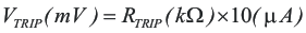
The trip level should be in the range of 30 mV to 200 mV over all operational temperature. The inductor current is monitored by the voltage between PGNDx pin and LLx pin. ITRIP has 4000ppm/°C temperature slope to compensate the temperature dependency of the RDS(on). PGNDx is used as the positive current sensing node so that PGNDx should be connected to the source terminal of the bottom MOSFET.
As the comparison is done during the OFF state, VTRIP sets valley level of the inductor current. Thus, the load current at over-current threshold, IOCP, can be calculated as follows:
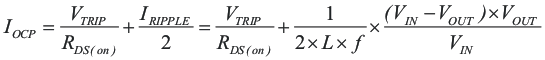
In an over-current condition, the current to the load exceeds the current to the output capacitor; thus the output voltage tends to fall off. Eventually, it will end up with crossing the under voltage protection threshold and shutdown.
4.3.8 Over/Under Voltage Protection
TPS53124 monitors a resistor divided feedback voltage to detect over and under voltage. When the feedback voltage becomes higher than 115% of the target voltage, the OVP comparator output goes high and the circuit latches as the high-side MOSFET driver OFF and the low-side MOSFET driver ON.
When the feedback voltage becomes lower than 70% of the target voltage, the UVP comparator output goes high and an internal UVP delay counter begins counting. After 30 μs, TPS53124 latches OFF both top and bottom MOSFET drivers, and shut off both drivers of another channel. This function is enabled approximately 2.0 ms.
4.3.9 UVLO Protection
TPS53124 has V5FILT Under Voltage Lock Out protection (UVLO). When the V5FILT voltage is lower than UVLO threshold voltage TPS53124 is shut off. This is non-latch protection.
4.3.10 Thermal Shutdown
TPS53124 monitors the temperature of itself. If the temperature exceeds the threshold value (typically 150°C), the switchers will be shut off as both DRVH and DRVL at low, the output discharge function enabled. Then TPS53124 is shut off. This is non-latch protection.
4.4 Device Functional Modes
The TPS53124 has two operating modes. The TPS53124 is in shut down mode when the EN1 and EN2 pins are low. When the EN1 and EN2 pins is pulled high, the TPS53124 enters the normal operating mode.