SLUSCD4B March   2017  – May 2018 TPS543C20

PRODUCTION DATA.  

  1. Features
  2. Applications
  3. Description
    1.     Device Images
      1.      Simplified Schematic
  4. Revision History
  5. Device Comparison Table
  6. Pin Configuration and Functions
    1.     Pin Functions
  7. Specifications
    1. 7.1 Absolute Maximum Ratings
    2. 7.2 ESD Ratings
    3. 7.3 Recommended Operating Conditions
    4. 7.4 Thermal Information
    5. 7.5 Electrical Characteristics
    6. 7.6 Typical Characteristics
  8. Detailed Description
    1. 8.1 Overview
    2. 8.2 Functional Block Diagram
    3. 8.3 Feature Description
    4. 8.4 Device Functional Modes
      1. 8.4.1  Soft-Start Operation
      2. 8.4.2  Input and VDD Undervoltage Lockout (UVLO) Protection
      3. 8.4.3  Power Good and Enable
      4. 8.4.4  Voltage Reference
      5. 8.4.5  Prebiased Output Start-up
      6. 8.4.6  Internal Ramp Generator
        1. 8.4.6.1 Ramp Selections
      7. 8.4.7  Switching Frequency
      8. 8.4.8  Clock Sync Point Selection
      9. 8.4.9  Synchronization and Stackable Configuration
      10. 8.4.10 Dual-Phase Stackable Configurations
        1. 8.4.10.1 Configuration 1: Master Sync Out Clock-to-Slave
        2. 8.4.10.2 Configuration 2: Master and Slave Sync to External System Clock
      11. 8.4.11 Operation Mode
      12. 8.4.12 API/BODY Brake
      13. 8.4.13 Sense and Overcurrent Protection
        1. 8.4.13.1 Low-Side MOSFET Overcurrent Protection
        2. 8.4.13.2 High-Side MOSFET Overcurrent Protection
      14. 8.4.14 Output Overvoltage and Undervoltage Protection
      15. 8.4.15 Overtemperature Protection
      16. 8.4.16 RSP/RSN Remote Sense Function
      17. 8.4.17 Current Sharing
      18. 8.4.18 Loss of Synchronization
  9. Application and Implementation
    1. 9.1 Application Information
    2. 9.2 Typical Application: TPS543C20 Stand-alone Device
      1. 9.2.1 Design Requirements
      2. 9.2.2 Detailed Design Procedure
        1. 9.2.2.1 Custom Design With WEBENCH® Tools
        2. 9.2.2.2 Switching Frequency Selection
        3. 9.2.2.3 Inductor Selection
        4. 9.2.2.4 Input Capacitor Selection
        5. 9.2.2.5 Bootstrap Capacitor Selection
        6. 9.2.2.6 BP Pin
        7. 9.2.2.7 R-C Snubber and VIN Pin High-Frequency Bypass
        8. 9.2.2.8 Output Capacitor Selection
          1. 9.2.2.8.1 Response to a Load Transient
          2. 9.2.2.8.2 Ramp Selection Design to Ensure Stability
      3. 9.2.3 Application Curves
    3. 9.3 System Example
      1. 9.3.1 Two-Phase Stackable
        1. 9.3.1.1 Application Curves
  10. 10Power Supply Recommendations
  11. 11Layout
    1. 11.1 Layout Guidelines
    2. 11.2 Layout Example
    3. 11.3 Package Size, Efficiency and Thermal Performance
  12. 12Device and Documentation Support
    1. 12.1 Device Support
      1. 12.1.1 Development Support
        1. 12.1.1.1 Custom Design With WEBENCH® Tools
      2. 12.1.2 Documentation Support
        1. 12.1.2.1 Related Documentation
    2. 12.2 Receiving Notification of Documentation Updates
    3. 12.3 Community Resources
    4. 12.4 Trademarks
    5. 12.5 Electrostatic Discharge Caution
    6. 12.6 Glossary
  13. 13Mechanical, Packaging, and Orderable Information

Package Options

Mechanical Data (Package|Pins)
Thermal pad, mechanical data (Package|Pins)
Orderable Information

Typical Characteristics

VIN = VDD = 12 V, TA = 25°C, RRT = 40.2 kΩ, TA= 25°C (unless otherwise specified)
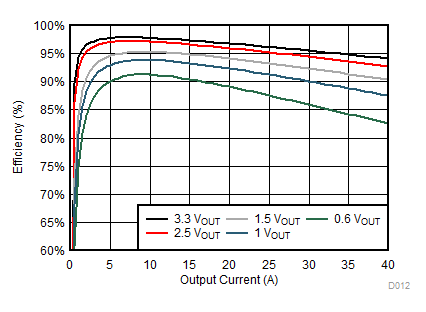
TPS543C20 D012_SLUSCD4.gif
VIN = 5 V 500 kHz 25°C
Figure 1. Efficiency vs Output Current
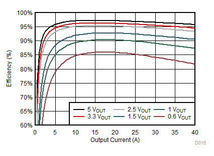
TPS543C20 D016_SLUSCD4.gif
VIN = 12 V 500 kHz 25°C
Figure 3. Efficiency vs Output Current
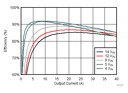
TPS543C20 D020_SLUSCD4.gif
VOUT = 1 V 1 MHz 25°C
Figure 5. Efficiency vs Output Current
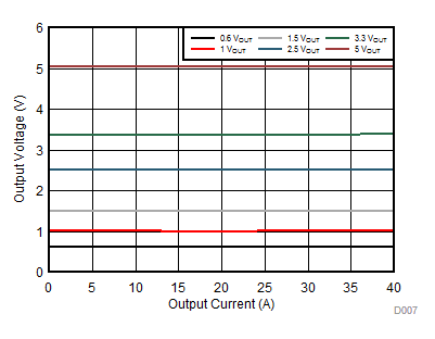
TPS543C20 D007_SLUSCD4.gif
VIN = 12 V 500 kHz 25°C
Figure 7. Output Voltage vs Output Current
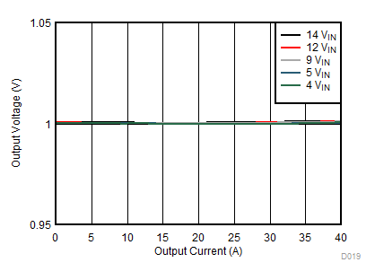
TPS543C20 D019_SLUSCD4.gif
VOUT = 1 V 1 MHz 25°C
Figure 9. Output Voltage vs Output Current
TPS543C20 tc003_sluscd4.gifFigure 11. Output Voltage Start-Up and Shutdown
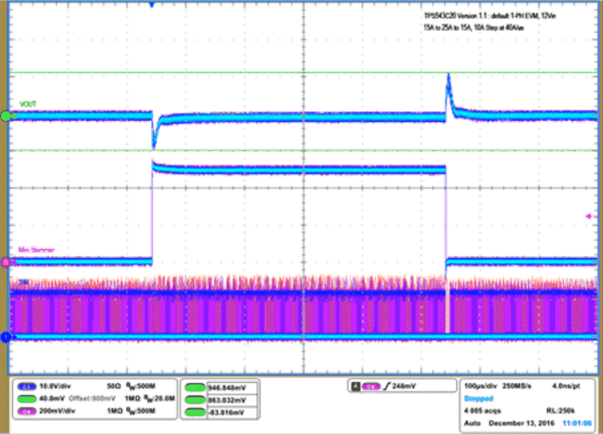
TPS543C20 tc006_sluscd4.gif
15 A to 25 A to 15 A, 10-A Step at 40 A/µs
Figure 13. Output Voltage Transient Response
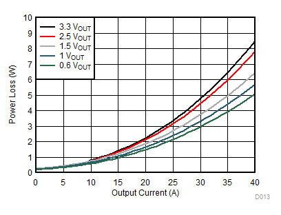
TPS543C20 D013_SLUSCD4.gif
VIN = 5 V 500 kHz 25°C
Figure 2. Power Loss vs Output Current
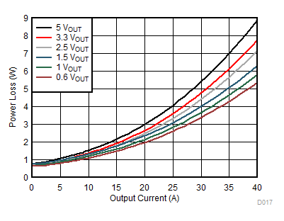
TPS543C20 D017_SLUSCD4.gif
VIN = 12 V 500 kHz 25°C
Figure 4. Power Loss vs Output Current
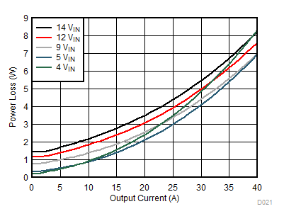
TPS543C20 D021_SLUSCD4.gif
VOUT = 1 V 1 MHz 25°C
Figure 6. Power Loss vs Output Current
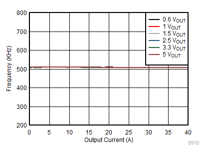
TPS543C20 D010_SLUSCD4.gif
VIN = 12 V 500 kHz 25°C
Figure 8. Switching Frequency vs Output Current
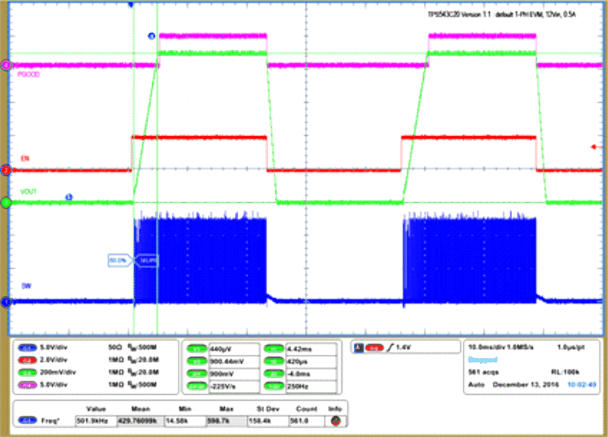
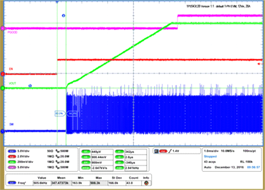
TPS543C20 tc001_sluscd4.gifFigure 10. Start-Up From EN
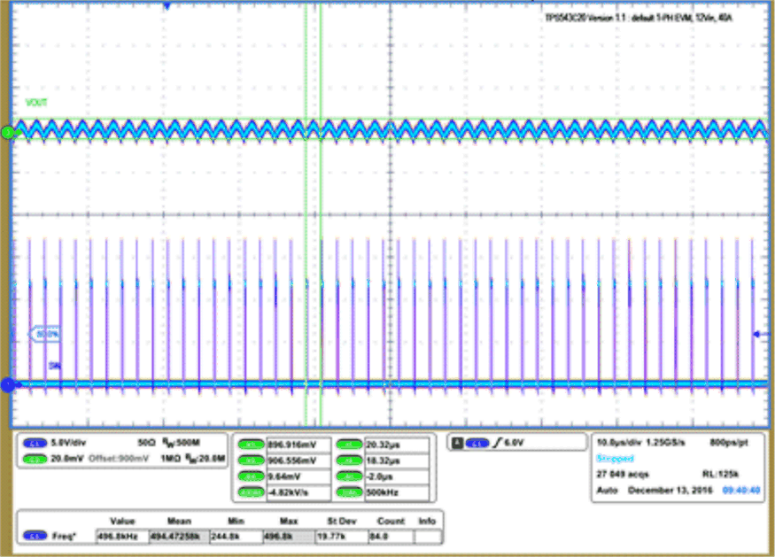
TPS543C20 tc005_sluscd4.gifFigure 12. Output Voltage Ripple at Steady State