SLVS757E March 2007 – July 2022 TPS5450
PRODUCTION DATA
- 1 Features
- 2 Applications
- 3 Description
- 4 Revision History
- 5 Pin Configuration and Functions
- 6 Specifications
-
7 Detailed Description
- 7.1 Overview
- 7.2 Functional Block Diagram
- 7.3
Feature Description
- 7.3.1 Oscillator Frequency
- 7.3.2 Voltage Reference
- 7.3.3 Enable (ENA) and Internal Slow-Start
- 7.3.4 Undervoltage Lockout (UVLO)
- 7.3.5 Boost Capacitor (BOOT)
- 7.3.6 Output Feedback (VSENSE) and Internal Compensation
- 7.3.7 Voltage Feed-Forward
- 7.3.8 Pulse-Width-Modulation (PWM) Control
- 7.3.9 Overcurrent Limiting
- 7.3.10 Overvoltage Protection
- 7.3.11 Thermal Shutdown
- 7.4 Device Functional Modes
-
8 Application and Implementation
- 8.1 Application Information
- 8.2
Typical Application
- 8.2.1 Design Requirements
- 8.2.2 Detailed Design Procedure
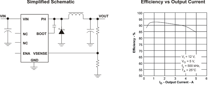
- 8.2.3 Application Curves
- 9 Power Supply Recommendations
- 10Layout
- 11Device and Documentation Support
- 12Mechanical, Packaging, and Orderable Information
Package Options
Refer to the PDF data sheet for device specific package drawings
Mechanical Data (Package|Pins)
- DDA|8
Thermal pad, mechanical data (Package|Pins)
- DDA|8
Orderable Information
3 Description
The TPS5450 is a high-output-current PWM converter that integrates a low-resistance, high-side N-channel MOSFET. Included on the substrate with the listed features are a high-performance voltage error amplifier that provides tight voltage regulation accuracy under transient conditions; an undervoltage-lockout circuit to prevent start-up until the input voltage reaches 5.5 V; an internally set slow-start circuit to limit inrush currents; and a voltage feed-forward circuit to improve the transient response. Using the ENA pin, shutdown supply current is reduced to 18 μA typically. Other features include an active-high enable, overcurrent limiting, overvoltage protection and thermal shutdown. To reduce design complexity and external component count, the TPS5450 feedback loop is internally compensated.
The TPS5450 device is available in a thermally-enhanced, 8-pin SOIC PowerPAD package. TI provides evaluation modules and software tool to aid in achieving high-performance power supply designs to meet aggressive equipment development cycles.
| PART NUMBER | PACKAGE | BODY SIZE (NOM) |
|---|---|---|
| TPS5450 | HSOP (8) | 4.89 mm × 3.90 mm |