SLVS757E March 2007 – July 2022 TPS5450
PRODUCTION DATA
- 1 Features
- 2 Applications
- 3 Description
- 4 Revision History
- 5 Pin Configuration and Functions
- 6 Specifications
-
7 Detailed Description
- 7.1 Overview
- 7.2 Functional Block Diagram
- 7.3
Feature Description
- 7.3.1 Oscillator Frequency
- 7.3.2 Voltage Reference
- 7.3.3 Enable (ENA) and Internal Slow-Start
- 7.3.4 Undervoltage Lockout (UVLO)
- 7.3.5 Boost Capacitor (BOOT)
- 7.3.6 Output Feedback (VSENSE) and Internal Compensation
- 7.3.7 Voltage Feed-Forward
- 7.3.8 Pulse-Width-Modulation (PWM) Control
- 7.3.9 Overcurrent Limiting
- 7.3.10 Overvoltage Protection
- 7.3.11 Thermal Shutdown
- 7.4 Device Functional Modes
-
8 Application and Implementation
- 8.1 Application Information
- 8.2
Typical Application
- 8.2.1 Design Requirements
- 8.2.2 Detailed Design Procedure
- 8.2.3 Application Curves
- 9 Power Supply Recommendations
- 10Layout
- 11Device and Documentation Support
- 12Mechanical, Packaging, and Orderable Information
Package Options
Refer to the PDF data sheet for device specific package drawings
Mechanical Data (Package|Pins)
- DDA|8
Thermal pad, mechanical data (Package|Pins)
- DDA|8
Orderable Information
8.2.2.9.2 Internal Compensation Network
The design equations given in the example circuit can be used to generate circuits using the TPS5450. These designs are based on certain assumptions and will tend to always select output capacitors within a limited range of ESR values. If a different capacitor type is desired, it may be possible to fit one to the internal compensation of the TPS5450. Equation 15 gives the nominal frequency response of the internal voltage-mode type III compensation network:
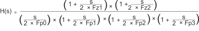
where
- Fp0 = 2165 Hz, Fz1 = 2170 Hz, Fz2 = 2590 Hz
- Fp1 = 24 kHz, Fp2 = 54 kHz, Fp3 = 440 kHz
- Fp3 represents the non-ideal parasitics effect.
Using this information along with the desired output voltage, feed-forward gain and output filter characteristics, the closed-loop transfer function can be derived.