SLUSDL8B December 2019 – April 2021 TPS563202
PRODUCTION DATA
- 1 Features
- 2 Applications
- 3 Description
- 4 Revision History
- 5 Pin Configuration and Functions
- 6 Specifications
- 7 Detailed Description
- 8 Application and Implementation
- 9 Layout
- 10Device and Documentation Support
- 11Mechanical, Packaging, and Orderable Information
Package Options
Mechanical Data (Package|Pins)
- DRL|6
Thermal pad, mechanical data (Package|Pins)
Orderable Information
8.2.3 Application Curves
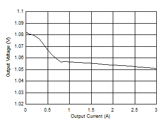 Figure 8-2 Load Regulation with different loading
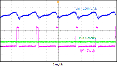 Figure 8-4 Input
Voltage Ripple
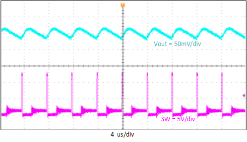 Figure 8-6 Output Voltage Ripple, Iout = 0.3 A
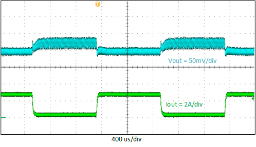 Figure 8-8 Transient Load Response, 0.3 to 2.7 A
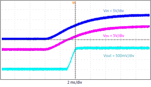 Figure 8-10 Start
Up Relative to VIN
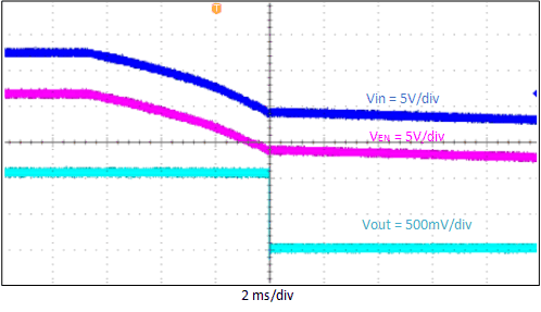 Figure 8-12 Shutdown Relative to VIN
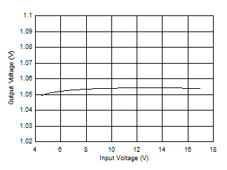 Figure 8-3 Load Regulation with different input voltage
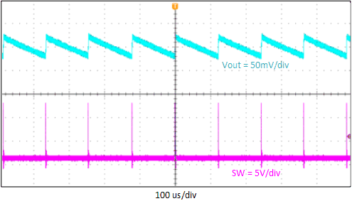 Figure 8-5 Output Voltage Ripple, 10 mA
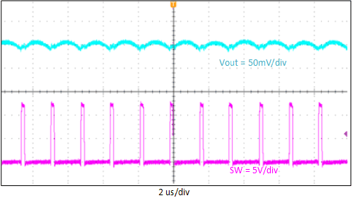 Figure 8-7 Output Voltage Ripple, Iout = 3 A
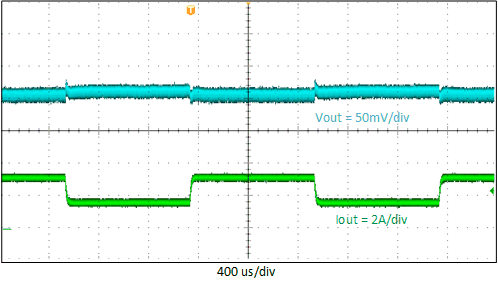 Figure 8-9 Transient Load Response, 1.5 to 3 A
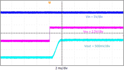 Figure 8-11 Start-Up Relative to EN
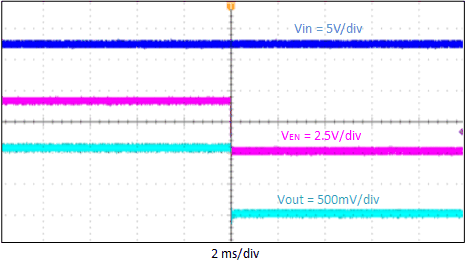 Figure 8-13 Shutdown Relative to EN