SLUSDL0A January 2020 – March 2020 TPS59603-Q1
PRODUCTION DATA.
- 1 Features
- 2 Applications
- 3 Description
- 4 Revision History
- 5 Pin Configuration and Functions
- 6 Specifications
- 7 Detailed Description
- 8 Power Supply Recommendations
- 9 Layout
- 10Device and Documentation Support
- 11Mechanical, Packaging, and Orderable Information
Package Options
Mechanical Data (Package|Pins)
- DSG|8
Thermal pad, mechanical data (Package|Pins)
- DSG|8
Orderable Information
9.2 Layout Recommendation
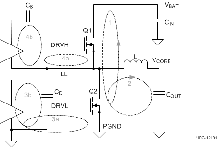
Figure 17 above shows the primary current loops in each phase, numbered in order of importance.
The most important loop to minimize the area of is loop 1, the path from the input capacitor through the high and low-side FETs, and back to the capacitor through ground.
Loop 2 is from the inductor through the output capacitor, ground, and Q2. The layout of the low-side gate drive (Loops 3a and 3b) is important. The guidelines for the gate drive layout are:
- Make the low-side gate drive length as short as possible (1 inch or less preferred).
- Make the DRVL width to length ratio of 1:10, wider (1:5) if possible.
- If changing layers is necessary, use at least two vias.
 Figure 17. Layout recommendations to minimize major Current loops