SLVS538B NOVEMBER 2004 – December 2014 TPS61060 , TPS61061 , TPS61062
PRODUCTION DATA.
- 1 Features
- 2 Applications
- 3 Description
- 4 Revision History
- 5 Device Comparison Table
- 6 Pin Configuration and Functions
- 7 Specifications
- 8 Detailed Description
- 9 Application and Implementation
- 10Power Supply Recommendations
- 11Layout
- 12Device and Documentation Support
- 13Mechanical, Packaging, and Orderable Information
Package Options
Refer to the PDF data sheet for device specific package drawings
Mechanical Data (Package|Pins)
- YZF|8
- DRB|8
Thermal pad, mechanical data (Package|Pins)
- DRB|8
Orderable Information
9 Application and Implementation
NOTE
Information in the following applications sections is not part of the TI component specification, and TI does not warrant its accuracy or completeness. TI’s customers are responsible for determining suitability of components for their purposes. Customers should validate and test their design implementation to confirm system functionality.
9.1 Application Information
The TPS6106x is designed to driver up to five LEDs in series with constant current output. The device, which operates in peak current mode PWM control, has a switch peak current limit of 325-mA minimum and internal loop compensation. The switching frequency is fixed at 1 MHz, and the input voltage range is 2.7 to 6.0 V. The following section provides a step-by-step design approach for configuring the TPS61060 to power two white LEDs in series.
9.2 Typical Application
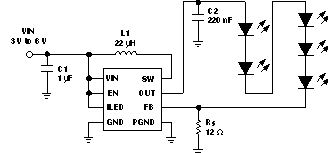 Figure 10. TPS61062 Powering Five White LEDs
9.2.1 Design Requirements
| PARAMETER | VALUE |
|---|---|
| Input Voltage | 3 V to 6 V |
| Output Current | 20 mA |
9.2.2 Detailed Design Procedure
9.2.2.1 Inductor Selection
The device requires typically a 22-µH or 10-µH inductance. When selecting the inductor, the inductor saturation current should be rated as high as the peak inductor current at maximum load, and respectively, maximum LED current. Because of the special control loop design, the inductor saturation current does not need to be rated for the maximum switch current of the converter. The maximum converter switch current usually is not reached even when the LED current is pulsed by applying a PWM signal to the enable pin. The maximum inductor peak current, as well as LED current, is calculated as:

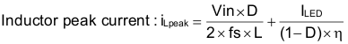
with:
fs = Switching frequency (1 MHz typical)
L = Inductor value
η = Estimated converter efficiency (0.75)
Isw = Minimum N-channel MOSFET current limit (325 mA)
Using the expected converter efficiency is a simple approach to calculate maximum possible LED current as well as peak inductor current. The efficiency can be estimated by taking the efficiency numbers out of the provided efficiency curves or to use a worst-case assumption for the expected efficiency, for example, 75%.
9.2.2.2 Efficiency
The overall efficiency of the application depends on the specific application conditions and mainly on the selection of the inductor. A physically smaller inductor usually shows lower efficiency due to higher switching losses of the inductor (core losses, proximity losses, skin effect losses). A trade-off between physical inductor size and overall efficiency has to be made. The efficiency can typically vary around ±5% depending on the selected inductor. Figure 2 to Figure 7 can be used as a guideline for the application efficiency. These curves show the typical efficiency with a 22-µH inductor (Murata Electronics LQH32CN220K23). Figure 11 shows a basic setup where the efficiency is taken/measured as:
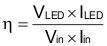
Table 3. Inductor Selection
| INDUCTOR VALUE | COMPONENT SUPPLIER | DIMENSIONS |
|---|---|---|
| 10 µH | TDK VLF3012AT-100MR49 | 2.6 mm × 2.8 mm × 1.2 mm |
| 10 µH | Murata LQH32CN100K53 | 3.2 mm × 2.5 mm × 1.55 mm |
| 10 µH | Murata LQH32CN100K23 | 3.2 mm × 2.5 mm × 2.0 mm |
| 22 µH | TDK VLF3012AT-220MR33 | 2.6 mm × 2.8 mm × 1.2 mm |
| 22 µH | Murata LQH32CN220K53 | 3.2 mm × 2.5 mm × 1.55 mm |
| 22 µH | Murata LQH32CN220K23 | 3.2 mm × 2.5 mm × 2.0 mm |
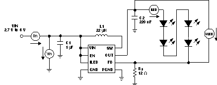 Figure 11. Efficiency Measurement Setup
9.2.2.3 Output Capacitor Selection
The device is designed to operate with a fairly wide selection of ceramic output capacitors. The selection of the output capacitor value is a trade-off between output voltage ripple and capacitor cost and form factor. In general, capacitor values of 220 nF up to 4.7 µF can be used. When using a 220-nF output capacitor, it is recommended to use X5R or X7R dielectric material to avoid the output capacitor value falling far below 220 nF over temperature and applied voltage. For systems with wireless or RF sections, EMI is always a concern. To minimize the voltage ripple in the LED string and board traces, the output capacitor needs to be connected directly from the OUT pin of the device to ground rather than across the LEDs. A larger output capacitor value reduces the output voltage ripple. Table 4 shows possible input and/or output capacitors.
9.2.2.4 Input Capacitor Selection
For good input voltage filtering, low ESR ceramic capacitors are recommended. A 1-µF ceramic input capacitor is sufficient for most of the applications. For better input voltage filtering and EMI reduction, this value can be increased. The input capacitor should be placed as close as possible to the input pin of the converter. Table 4 shows possible input and/or output capacitors.
Table 4. Capacitor Selection
| CAPACITOR | VOLTAGE RATING | FORM FACTOR | COMPONENT SUPPLIER(1) | COMMENTS |
|---|---|---|---|---|
| INPUT CAPACITOR | ||||
| 1 µF | 10 V | 0603 | Tayo Yuden LMK107BJ105 | |
| OUTPUT CAPACITOR | ||||
| 220 nF | 16 V | 0603 | Tayo Yuden EMK107BJ224 | TPS61060 |
| 220 nF | 50 V | 0805 | Tayo Yuden UMK212BJ224 | TPS61060/61/62 |
| 470 nF | 35 V | 0805 | Tayo Yuden GMK212BJ474 | TPS61060/61/62 |
| 1 µF | 16 V | 0805 | Tayo Yuden EMK212BJ105 | TPS61060 |
| 1 µF | 35 V | 1206 | Tayo Yuden GMK316BJ105 | TPS61060/61/62 |
| 1 µF | 25 V | 1206 | TDK C3216X7R1E105 | TPS61060/61/62 |
9.2.3 Application Curves
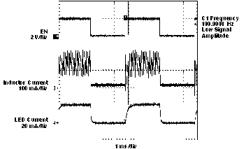
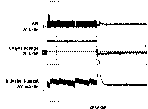 Figure 14. Short-Circuit Protection
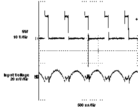 Figure 16. Input Voltage Ripple
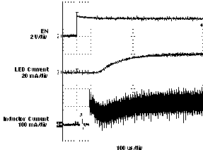 Figure 13. Soft-Start Operation
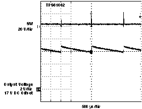 Figure 15. Overvoltage Protection
9.3 System Examples
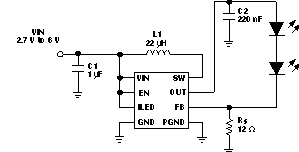 Figure 17. TPS61060 Powering Two White LEDs
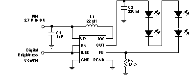
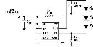 Figure 18. TPS61060 Powering Three White LEDs
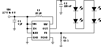 Figure 19. TPS61061 Powering Four White LEDs
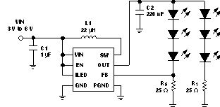 Figure 20. TPS61060 Powering Six White LEDs