SLVS538B NOVEMBER 2004 – December 2014 TPS61060 , TPS61061 , TPS61062
PRODUCTION DATA.
- 1 Features
- 2 Applications
- 3 Description
- 4 Revision History
- 5 Device Comparison Table
- 6 Pin Configuration and Functions
- 7 Specifications
- 8 Detailed Description
- 9 Application and Implementation
- 10Power Supply Recommendations
- 11Layout
- 12Device and Documentation Support
- 13Mechanical, Packaging, and Orderable Information
Package Options
Refer to the PDF data sheet for device specific package drawings
Mechanical Data (Package|Pins)
- YZF|8
- DRB|8
Thermal pad, mechanical data (Package|Pins)
- DRB|8
Orderable Information
7 Specifications
7.1 Absolute Maximum Ratings(1)
over operating free-air temperature range (unless otherwise noted)| MIN | MAX | UNIT | ||
|---|---|---|---|---|
| VIN(2) | Supply voltages on pin | –0.3 | 7 | V |
| EN, ILED, FB(2) | Voltages on pins | –0.3 | 7 | V |
| OUT(2) | Voltage on pin | 33 | V | |
| SW(2) | Voltage on pin | 33 | V | |
| Operating junction temperature | –40 | 150 | °C | |
| Lead temperature (soldering, 10 s) | 260 | °C | ||
| Tstg | Storage temperature | –55 | 150 | °C |
(1) Stresses beyond those listed under Absolute Maximum Ratings may cause permanent damage to the device. These are stress ratings only, and functional operation of the device at these or any other conditions beyond those indicated under Recommended Operating Conditions is not implied. Exposure to absolute-maximum-rated conditions for extended periods may affect device reliability.
(2) All voltage values are with respect to network ground terminal.
7.2 ESD Ratings
| VALUE | UNIT | |||
|---|---|---|---|---|
| V(ESD) | Electrostatic discharge | Human body model (HBM), per ANSI/ESDA/JEDEC JS-001(1) | ±4000 | V |
| Charged-device model (CDM), per JEDEC specification JESD22-C101(2) | ±750 | |||
(1) JEDEC document JEP155 states that 500-V HBM allows safe manufacturing with a standard ESD control process.
(2) JEDEC document JEP157 states that 250-V CDM allows safe manufacturing with a standard ESD control process.
7.3 Recommended Operating Conditions
| MIN | TYP | MAX | UNIT | ||
|---|---|---|---|---|---|
| VI | Input voltage range | 2.7 | 6.0 | V | |
| L | Inductor(1) | 22 | µH | ||
| CI | Input capacitor(1) | 1 | µF | ||
| CO | Output capacitor(1) | 0.22 | 1 | µF | |
| TA | Operating ambient temperature | -40 | 85 | °C | |
| TJ | Operating junction temperature | -40 | 125 | °C |
(1) Refer to application section for further information.
7.4 Thermal Information
| THERMAL METRIC(1) | TPS6106x | UNIT | ||
|---|---|---|---|---|
| DRB | YZF | |||
| 8 PINS | ||||
| RθJA | Junction-to-ambient thermal resistance | 47.6 | 120.8 | °C/W |
| RθJC(top) | Junction-to-case (top) thermal resistance | 54.1 | 0.7 | |
| RθJB | Junction-to-board thermal resistance | 23.2 | 59.4 | |
| ψJT | Junction-to-top characterization parameter | 1.0 | 2.2 | |
| ψJB | Junction-to-board characterization parameter | 23.4 | 59.4 | |
| RθJC(bot) | Junction-to-case (bottom) thermal resistance | 7.1 | n/a | |
(1) For more information about traditional and new thermal metrics, see the IC Package Thermal Metrics application report, SPRA953.
7.5 Electrical Characteristics
Vin = 3.6 V, EN = VIN, TA= –40°C to 85°C, typical values are at TA = 25°C (unless otherwise noted)| PARAMETER | TEST CONDITIONS | MIN | TYP | MAX | UNIT | |
|---|---|---|---|---|---|---|
| SUPPLY CURRENT | ||||||
| VIN | Input voltage range | 2.7 | 6 | V | ||
| IQ | Operating quiescent current into Vin | Device not switching | 1 | mA | ||
| ISD | Shutdown current | EN = GND | 1 | 10 | µA | |
| VUVLO | Undervoltage lockout threshold | VIN falling | 1.65 | 1.8 | V | |
| VHYS | Undervoltage lockout hysteresis | 50 | mV | |||
| ENABLE AND ILED | ||||||
| VEN | Enable high-level voltage | VIN = 2.7 V to 6 V | 1.2 | V | ||
| VEN | Enable low-level voltage | VIN = 2.7 V to 6 V | 0.4 | V | ||
| REN | Enable pulldown resistor | 200 | 300 | kΩ | ||
| tshtdn | Enable-to-shutdown delay (1) | EN = high to low | 50 | ms | ||
| tPWML | PWM low-level signal time (1) | PWM signal applied to EN | 25 | ms | ||
| VILED | ILED high-level voltage | VIN = 2.7 V to 6 V | 1.2 | V | ||
| VILED | ILED low-level voltage | VIN = 2.7 V to 6 V | 0.4 | V | ||
| IILED | ILED input leakage current | ILED = GND or VIN | 0.1 | 3 | µA | |
| DAC resolution | 5 Bit | 15.6 | mV | |||
| tup | Increase feedback voltage one step | ILED = high to low | 1 | 75 | µs | |
| tdown | Decrease feedback voltage one step | ILED = high to low | 180 | 300 | µs | |
| tdelay | Delay time between up/down steps | ILED = low to high | 1.5 | µs | ||
| toff | Digital programming off, VFB = 500 mV | ILED = high to low | 720 | µs | ||
| FEEDBACK FB | ||||||
| IFB | Feedback input bias current | VFB = 500 mV | 1 | 1.5 | µA | |
| VFB | Feedback regulation voltage | ILED = GND, after start-up | 485 | 500 | 515 | mV |
| VFB | Feedback regulation voltage | ILED = High, after start-up | 240 | 250 | 260 | mV |
| POWER SWITCH SYNCHRONOUS RECTIFIER AND CURRENT LIMIT (SW) | ||||||
| rDS(ON) | P-channel MOSFET on-resistance | VO = 10 V, Isw = 10 mA | 2.5 | 3.7 | Ω | |
| RDS(ON) | N-channel MOSFET on-resistance | VIN = VGS = 3.6 V, Isw = 100 mA | 0.6 | 0.9 | Ω | |
| N-channel MOSFET on-resistance | VIN = VGS = 2.7 V, Isw = 100 mA | 0.7 | 1.0 | Ω | ||
| Iswleak | Switch leakage current(2) | VIN = VSW= 6 V, VOUT = GND, EN = GND |
0.1 | 2 | µA | |
| ISW | N-Channel MOSFET current limit | VO = 10 V | 325 | 400 | 475 | mA |
| OSCILLATOR | ||||||
| fs | Switching frequency | 0.8 | 1.0 | 1.2 | MHz | |
| OUTPUT | ||||||
| Vovp | Output overvoltage protection | VO rising; TPS61060 | 14 | 14.5 | 16 | V |
| Vovp | Output overvoltage protection | VO rising; TPS61061 | 18 | 18.5 | 19.8 | V |
| Vovp | Output overvoltage protection | VO rising; TPS61062 | 22.2 | 23.5 | 25 | V |
| Vovp | Output overvoltage protection hysteresis | TPS61060/61/62, VO falling | 0.7 | V | ||
| Vo | Output voltage threshold for short-circuit detection | VO falling | VIN–0.7 | V | ||
| Vo | Output voltage threshold for short-circuit detection | VO rising | VIN–0.3 | V | ||
| Ipre | Precharge current and short-circuit current | Start-up, EN = low to high, OUT = GND |
mA | |||
| VIN = 6 V | 180 | |||||
| VIN = 3.6 V | 95 | |||||
| VIN = 2.7 V | 65 | |||||
| D | Maximum duty cycle | 95% | ||||
(1) A PWM low signal applied to EN for a time (≥25 ms) could cause a device shutdown. After a period of ≥50 ms the device definitely enters shutdown mode.
(2) The switch leakage current includes the leakage current of both internal switches, which is the leakage current from SW to ground, and from SW to VOUT, with VIN = VSW.
7.6 Typical Characteristics
Table 1. Table of Graphs
| FIGURE | ||
|---|---|---|
| Efficiency (η) | vs LED current; 2 LEDs, ILED = high | Figure 1 |
| vs LED current; 3 LEDs, ILED = low | Figure 2 | |
| vs LED current; 3 LEDs, ILED = high | Figure 3 | |
| vs LED current; 4 LEDs, ILED = low | Figure 4 | |
| vs LED current; 4 LEDs, ILED = high | Figure 5 | |
| vs LED current; 5 LEDs, ILED = high | Figure 6 | |
| Digital brightness control | Feedback voltage vs ILED programming step | Figure 7 |
| LED current | vs PWM duty cycle | Figure 8 |
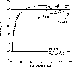 Figure 1. Efficiency vs LED Current
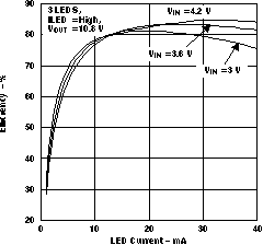 Figure 3. Efficiency vs LED Current
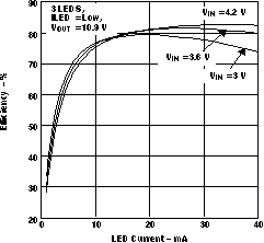 Figure 2. Efficiency vs LED Current
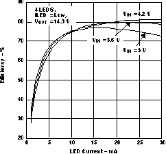 Figure 4. Efficiency vs LED Current
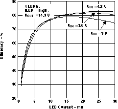 Figure 5. Efficiency vs LED Current
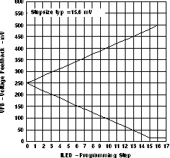
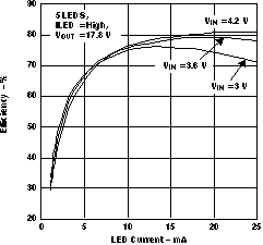 Figure 6. Efficiency vs LED Current
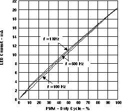 Figure 8. LED Current vs PWM Duty Cycle