SLVS538B NOVEMBER 2004 – December 2014 TPS61060 , TPS61061 , TPS61062
PRODUCTION DATA.
- 1 Features
- 2 Applications
- 3 Description
- 4 Revision History
- 5 Device Comparison Table
- 6 Pin Configuration and Functions
- 7 Specifications
- 8 Detailed Description
- 9 Application and Implementation
- 10Power Supply Recommendations
- 11Layout
- 12Device and Documentation Support
- 13Mechanical, Packaging, and Orderable Information
Package Options
Refer to the PDF data sheet for device specific package drawings
Mechanical Data (Package|Pins)
- YZF|8
- DRB|8
Thermal pad, mechanical data (Package|Pins)
- DRB|8
Orderable Information
11 Layout
11.1 Layout Guidelines
As for all switching power supplies, the layout is an important step in the design, especially at high peak currents and switching frequencies. If the layout is not carefully done, the regulator might show noise problems and duty cycle jitter. The input capacitor should be placed as close as possible to the input pin for good input voltage filtering. The inductor should be placed as close as possible to the switch pin to minimize the noise coupling into other circuits. The output capacitor needs to be placed directly from the OUT pin to GND rather than across the LEDs. This reduces the ripple current in the trace to the LEDs. The GND pin must be connected directly to the PGND pin. When doing the PCB layout, the bold traces (Figure 22) should be routed first, as well as placement of the inductor, and input and output capacitors.
11.2 Layout Example
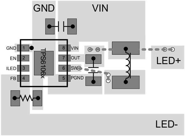 Figure 22. TPS6106x Layout Example
11.3 Thermal Considerations
The TPS6106x comes in a thermally enhanced QFN package. The package includes a thermal pad that improves the thermal capabilities of the package. Also see QFN/SON PCB Attachment application report (SLUA271). The thermal resistance junction-to-ambient RθJA of the QFN package greatly depends on the PCB layout. Using thermal vias and wide PCB traces improves the thermal resistance RθJA. The thermal pad must be soldered to the analog ground on the PCB.
For the NanoFree package, similar guidelines apply for the QFN package. The thermal resistance RθJA depends mainly on the PCB layout.