SLVS538B NOVEMBER 2004 – December 2014 TPS61060 , TPS61061 , TPS61062
PRODUCTION DATA.
- 1 Features
- 2 Applications
- 3 Description
- 4 Revision History
- 5 Device Comparison Table
- 6 Pin Configuration and Functions
- 7 Specifications
- 8 Detailed Description
- 9 Application and Implementation
- 10Power Supply Recommendations
- 11Layout
- 12Device and Documentation Support
- 13Mechanical, Packaging, and Orderable Information
Package Options
Refer to the PDF data sheet for device specific package drawings
Mechanical Data (Package|Pins)
- YZF|8
- DRB|8
Thermal pad, mechanical data (Package|Pins)
- DRB|8
Orderable Information
8 Detailed Description
8.1 Overview
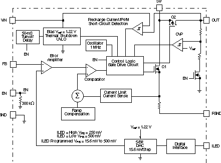
The TPS61060/61/62 family is a constant-frequency, PWM current-mode converter with an integrated N-channel MOSFET switch and synchronous P-channel MOSFET rectifier. The device operates in pulse width modulation (PWM) with a fixed switching frequency of 1 MHz. For an understanding of the device operation, refer the block diagram. The duty cycle of the converter is set by the error amplifier and the sawtooth ramp applied to the comparator. Because the control architecture is based on a current-mode control, a compensation ramp is added to allow stable operation for duty cycles larger than 50%. The converter is a fully integrated synchronous boost converter operating always in continuous conduction mode. This allows low noise operation and avoids ringing on the switch pin as it would be seen on a converter when entering discontinuous conduction mode.
8.2 Functional Block Diagram
8.3 Feature Description
8.3.1 Start-Up
To avoid high inrush current during start-up, special care is taken to control the inrush current. When the device is first enabled, the output capacitor is charged with a constant precharge current of typically 100 mA until the output voltage is typically 0.3 V below VIN. The device starts with a reduced analog controlled current limit for typically 40 µs. After this time, the device enters its normal regulation with full current limit. The fixed precharge current during start-up allows the device to start up without problems when driving LEDs because the LED only starts to conduct current when the forward voltage is reached. If, for any reason a resistive load is driven, the maximum start-up load current must be smaller, or equal to, the precharge current.
8.3.2 Short-Circuit Protection
The TPS6106x family has an advanced short-circuit protection in case the output of the device is shorted to ground. Because the device is configured as a current source even when the LEDs are shorted, the maximum current is controlled by the sense resistor Rs. As an additional safety feature, the TPS6106x series also protects the device and inductor when the output is shorted to ground. When the output is shorted to ground, the device enters precharge mode and limits the maximum current to typically 100 mA.
8.3.3 Overvoltage Protection (OVP)
As with any current source, the output voltage rises when the output gets high impedance or disconnected. To prevent the output voltage exceeding the maximum switch voltage rating (33 V) of the main switch, an overvoltage protection circuit is integrated. As soon as the output voltage exceeds the OVP threshold, the converter stops switching and the output voltage falls down. When the output voltage falls below the OVP threshold, the converter continues operation until the output voltage exceeds the OVP threshold again. To allow the use of inexpensive low-voltage output capacitors, the TPS6106x series has different OVP levels that must be selected according to the number of external LEDs and their maximum forward voltage.
8.3.4 Efficiency and Feedback Voltage
The feedback voltage has a direct effect on the converter efficiency. Because the voltage drop across the feedback resistor does not contribute to the output power (LED brightness), the lower the feedback voltage, the higher the efficiency. Especially when powering only three or less LEDs, the feedback voltage impacts the efficiency around 2% depending on the sum of the forward voltage of the LEDs. To take advantage of this, the ILED pin can be connected to VIN, setting the feedback voltage to 250 mV.
8.3.5 Undervoltage Lockout
An undervoltage lockout prevents mis-operation of the device at input voltages below typical 1.65 V. When the input voltage is below the undervoltage threshold, the device remains off and both internal MOSFETs are turned off providing isolation between input and output.
8.3.6 Thermal Shutdown
An internal thermal shutdown is implemented and turns off the internal MOSFETs when the typical junction temperature of 160°C is exceeded. The thermal shutdown has a hysteresis of typically 15°C.
8.4 Device Functional Modes
8.4.1 Enable PWM Dimming
The EN pin allows disabling and enabling of the device as well as brightness control of the LEDs by applying a PWM signal up to typically 1 kHz. When a PWM signal is applied, the LED current is turned on when the EN is high and off when EN is pulled low. Changing the PWM duty cycle therefore changes the LED brightness. To allow higher PWM frequencies on the enable pin, the device continues operation when a PWM signal is applied. As shown in the block diagram, the EN pin needs to be pulled low for at least 50 ms to fully turn the device off. The enable input pin has an internal 300-kΩ pulldown resistor to disable the device when this pin is floating.
8.4.2 Digital Brightness Control (ILED)
The ILED pin features a simple digital interface to allow digital brightness control. This can save processor power and battery life. Using the digital interface to control the LED brightness does not required a PWM signal all the time, and the processor can enter sleep mode if available. To save signal lines, the ILED pin can be connected to the enable pin to allow digital programming and enable/disable function at the same time with the same signal. Such a circuit is shown in Figure 9.
The ILED pin basically sets the feedback regulation voltage (VFB); thus, it sets the LED current. When the ILED pin is connected to GND, the digital brightness control is disabled and the feedback is regulated to VFB =
500 mV. When the ILED pin is pulled high, the digital brightness control is enabled starting at its midpoint where the feedback is regulated to VFB = 250 mV. The digital brightness control is implemented by adjusting the feedback voltage in digital steps with a typical maximum voltage of VFB = 500 mV. For this purpose, a 5-bit DAC is used giving 32 steps equal to a 15.6-mV change in feedback voltage per step. To increase or decrease the internal reference voltage, the ILED pin needs to be pulled low over time as outlined in Table 2 and specified in the electrical table. When the internal DAC is programmed to its highest or lowest value, it stays at this value until it gets programmed in the opposite direction again.
Table 2. Increase/Decrease Internal Reference Voltage
| FEEDBACK VOLTAGE | TIME | ILED LOGIC LEVEL |
|---|---|---|
| Increase | 1 µs to 75 µs | Low |
| Decrease | 180 µs to 300 µs | Low |
| Brightness control disabled | ≥550 µs | Low |
| Delay between steps | 1.5 µs | High |
Between each cycle the ILED pin needs to be pulled high for 1.5 µs.
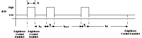 Figure 9. ILED Timing Diagram
Using the digital interface on the ILED pin allows simple implementation of a two-step brightness control by pulling the ILED either high or low. For full LED current with VFB = 500 mV, the ILED must be pulled low; to program half the LED current with VFB = 250 mV, the ILED pin must be pulled high.