SLVS992D September   2009  – April 2019 TPS61093

PRODUCTION DATA.  

  1. Features
  2. Applications
  3. Description
    1.     Device Images
      1.      Simplified Schematic
  4. Revision History
  5. Pin Configuration and Functions
    1.     Pin Functions
  6. Specifications
    1. 6.1 Absolute Maximum Ratings
    2. 6.2 ESD Ratings
    3. 6.3 Recommended Operating Conditions
    4. 6.4 Thermal Information
    5. 6.5 Electrical Characteristics
    6. 6.6 Typical Characteristics
  7. Detailed Description
    1. 7.1 Overview
    2. 7.2 Functional Block Diagram
    3. 7.3 Feature Description
      1. 7.3.1 Shutdown and Load Discharge
      2. 7.3.2 Overload and Overvoltage Protection
      3. 7.3.3 UVLO
      4. 7.3.4 Thermal Shutdown
    4. 7.4 Device Functional Modes
  8. Application and Implementation
    1. 8.1 Application Information
    2. 8.2 Typical Applications
      1. 8.2.1 15 V Output Boost Converter
        1. 8.2.1.1 Design Requirements
        2. 8.2.1.2 Detailed Design Procedure
          1. 8.2.1.2.1 Custom Design With WEBENCH® Tools
          2. 8.2.1.2.2 Output Program
          3. 8.2.1.2.3 Without Isolation FET
          4. 8.2.1.2.4 Start-Up
          5. 8.2.1.2.5 Switch Duty Cycle
          6. 8.2.1.2.6 Inductor Selection
          7. 8.2.1.2.7 Input and Output Capacitor Selection
          8. 8.2.1.2.8 Small Signal Stability
        3. 8.2.1.3 Application Curves
      2. 8.2.2 10 V, –10 V Dual Output Boost Converter
        1. 8.2.2.1 Design Requirements
        2. 8.2.2.2 Detailed Design Procedure
        3. 8.2.2.3 Application Curve
  9. Power Supply Recommendations
  10. 10Layout
    1. 10.1 Layout Guidelines
    2. 10.2 Layout Example
  11. 11Device and Documentation Support
    1. 11.1 Device Support
      1. 11.1.1 Third-Party Products Disclaimer
      2. 11.1.2 Development Support
        1. 11.1.2.1 Custom Design With WEBENCH® Tools
    2. 11.2 Receiving Notification of Documentation Updates
    3. 11.3 Community Resources
    4. 11.4 Trademarks
    5. 11.5 Electrostatic Discharge Caution
    6. 11.6 Glossary
  12. 12Mechanical, Packaging, and Orderable Information

Package Options

Mechanical Data (Package|Pins)
Thermal pad, mechanical data (Package|Pins)
Orderable Information

Application Curves

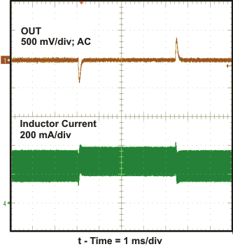
TPS61093 scope1_lvs992.gifFigure 10. 3.3 V to 3.6 V Line Transient Response
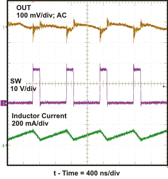
TPS61093 scope3_lvs992.gifFigure 12. PWM Control in CCM
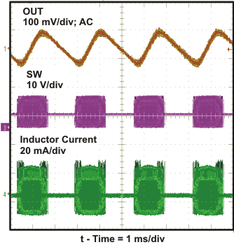
TPS61093 scope5_lvs992.gifFigure 14. Pulse Skip Mode at Light Load
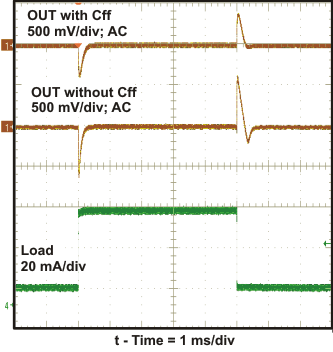
TPS61093 scope2_lvs992.gifFigure 11. 10 mA to 50 mA Load Transient Response
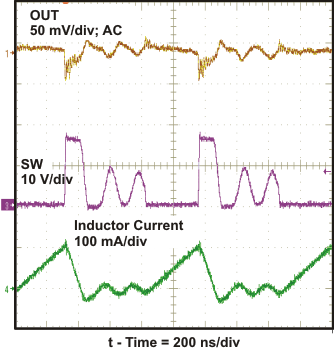
TPS61093 scope4_lvs992.gifFigure 13. PWM Control in DCM
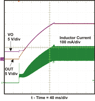
TPS61093 scope6_lvs992.gifFigure 15. Soft Start-Up