SLVS992D September 2009 – April 2019 TPS61093
PRODUCTION DATA.
- 1 Features
- 2 Applications
- 3 Description
- 4 Revision History
- 5 Pin Configuration and Functions
- 6 Specifications
- 7 Detailed Description
- 8 Application and Implementation
- 9 Power Supply Recommendations
- 10Layout
- 11Device and Documentation Support
- 12Mechanical, Packaging, and Orderable Information
Package Options
Mechanical Data (Package|Pins)
- DSK|10
Thermal pad, mechanical data (Package|Pins)
- DSK|10
Orderable Information
8.2.1.2.6 Inductor Selection
Because the selection of the inductor affects steady state operation, transient behavior, and loop stability, the inductor is the most important component in power regulator design. There are three important inductor specifications, inductor value, saturation current, and dc resistance. Considering inductor value alone is not enough.
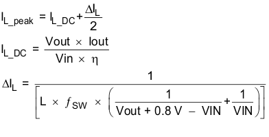
The saturation current of the inductor should be higher than the peak switch current as calculated in Equation 5.

where
- IL_peak = Peak switch current
- IL_DC = Inductor average current
- ΔIL = Inductor peak to peak current
- η = Estimated converter efficiency
Normally, it is advisable to work with an inductor peak-to-peak current of less than 30% of the average inductor current. A smaller ripple from a larger valued inductor reduces the magnetic hysteresis losses in the inductor and EMI. But in the same way, load transient response time is increased. Also, the inductor value should not be outside the 2.2 μH to 10 μH range in the recommended operating conditions table. Otherwise, the internal slope compensation and loop compensation components are unable to maintain small signal control loop stability over the entire load range. Table 3 lists the recommended inductor for the TPS61093.
Table 3. Recommended Inductors for the TPS61093
| PART NUMBER | L (μH) | DCR MAX (mΩ) | SATURATION CURRENT (A) | SIZE (L×W×H mm) | VENDOR |
|---|---|---|---|---|---|
| #A915_Y-4R7M | 4.7 | 45 | 1.5 | 5.2x5.2x3.0 | Toko |
| #A915_Y-100M | 10 | 90 | 1.09 | 5.2x5.2x3.0 | Toko |
| VLS4012-4R7M | 4.7 | 132 | 1.1 | 4.0x4.0x1.2 | TDK |
| VLS4012-100M | 10 | 240 | 0.82 | 4.0x4.0x1.2 | TDK |
| CDRH3D23/HP | 10 | 198 | 1.02 | 4.0x4.0x2.5 | Sumida |
| LPS5030-103ML | 10 | 127 | 1.4 | 5.0x5.0x3.0 | Coilcraft |