SLVS992D September   2009  – April 2019 TPS61093

PRODUCTION DATA.  

  1. Features
  2. Applications
  3. Description
    1.     Device Images
      1.      Simplified Schematic
  4. Revision History
  5. Pin Configuration and Functions
    1.     Pin Functions
  6. Specifications
    1. 6.1 Absolute Maximum Ratings
    2. 6.2 ESD Ratings
    3. 6.3 Recommended Operating Conditions
    4. 6.4 Thermal Information
    5. 6.5 Electrical Characteristics
    6. 6.6 Typical Characteristics
  7. Detailed Description
    1. 7.1 Overview
    2. 7.2 Functional Block Diagram
    3. 7.3 Feature Description
      1. 7.3.1 Shutdown and Load Discharge
      2. 7.3.2 Overload and Overvoltage Protection
      3. 7.3.3 UVLO
      4. 7.3.4 Thermal Shutdown
    4. 7.4 Device Functional Modes
  8. Application and Implementation
    1. 8.1 Application Information
    2. 8.2 Typical Applications
      1. 8.2.1 15 V Output Boost Converter
        1. 8.2.1.1 Design Requirements
        2. 8.2.1.2 Detailed Design Procedure
          1. 8.2.1.2.1 Custom Design With WEBENCH® Tools
          2. 8.2.1.2.2 Output Program
          3. 8.2.1.2.3 Without Isolation FET
          4. 8.2.1.2.4 Start-Up
          5. 8.2.1.2.5 Switch Duty Cycle
          6. 8.2.1.2.6 Inductor Selection
          7. 8.2.1.2.7 Input and Output Capacitor Selection
          8. 8.2.1.2.8 Small Signal Stability
        3. 8.2.1.3 Application Curves
      2. 8.2.2 10 V, –10 V Dual Output Boost Converter
        1. 8.2.2.1 Design Requirements
        2. 8.2.2.2 Detailed Design Procedure
        3. 8.2.2.3 Application Curve
  9. Power Supply Recommendations
  10. 10Layout
    1. 10.1 Layout Guidelines
    2. 10.2 Layout Example
  11. 11Device and Documentation Support
    1. 11.1 Device Support
      1. 11.1.1 Third-Party Products Disclaimer
      2. 11.1.2 Development Support
        1. 11.1.2.1 Custom Design With WEBENCH® Tools
    2. 11.2 Receiving Notification of Documentation Updates
    3. 11.3 Community Resources
    4. 11.4 Trademarks
    5. 11.5 Electrostatic Discharge Caution
    6. 11.6 Glossary
  12. 12Mechanical, Packaging, and Orderable Information

Package Options

Mechanical Data (Package|Pins)
Thermal pad, mechanical data (Package|Pins)
Orderable Information

Without Isolation FET

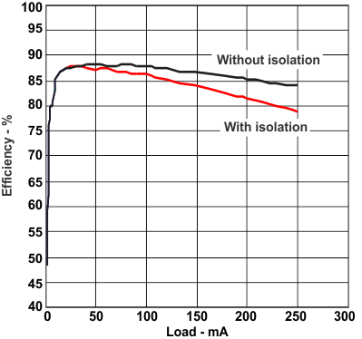
The efficiency of the TPS61093 can be improved by connecting the load to the VO pin instead of the OUT pin. The power loss in the isolation FET is then negligible, as shown in Figure 8. The tradeoffs when bypassing the isolation FET are:

  • Leakage path between input and output causes the output to be a diode drop below the input voltage when the IC is in shutdown
  • No overload circuit protection

When the load is connected to the VO pin, the output capacitor on the VO pin must be above 1 μF.
TPS61093 eff_ld_lvs992.gifFigure 8. Efficiency vs Load