SLVS577E March 2007 – December 2014 TPS61200 , TPS61201 , TPS61202
PRODUCTION DATA.
- 1 Features
- 2 Applications
- 3 Description
- 4 Typical Application
- 5 Revision History
- 6 Device Options
- 7 Pin Configuration and Functions
- 8 Specifications
- 9 Parameter Measurement Information
- 10Detailed Description
- 11Application and Implementation
- 12Power Supply Recommendations
- 13Layout
- 14Device and Documentation Support
- 15Mechanical, Packaging, and Orderable Information
Package Options
Mechanical Data (Package|Pins)
- DRC|10
Thermal pad, mechanical data (Package|Pins)
- DRC|10
Orderable Information
10 Detailed Description
10.1 Overview
The TPS6120x is a low input voltage synchronous boost converter family. The devices support 0.3-V to 5.5-V input voltage range, so can provide power supply solutions for products powered by either a single-cell, two-cell, or three-cell alkaline, NiCd or NiMH, or one-cell Li-Ion or Li-polymer battery. It is also used in fuel cell or solar cell powered devices where the capability of handling low input voltages is essential. The devices provide output currents of up to 600 mA at a 5-V output, while using a single-cell Li-Ion or Li-Polymer battery and discharges it down to 2.6 V. The boost converter is based on a fixed frequency, pulse-width-modulation (PWM) controller using synchronous rectification to obtain maximum efficiency. At low load currents, the converter enters the Power Save mode to maintain a high efficiency over a wide load current range. The Power Save mode can be disabled, forcing the converter to operate at a fixed switching frequency. The average input current is limited to a maximum value of 1500 mA. The output voltage is programmed by an external resistor divider, or is fixed internally on the chip. The converter can be disabled to minimize battery drain. During shutdown, the load is completely disconnected from the battery.
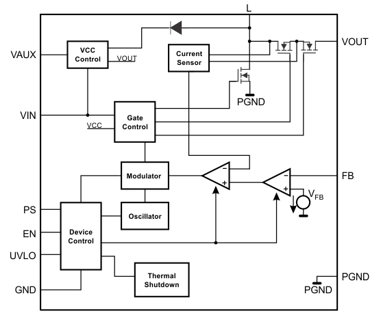
10.2 Functional Block Diagram
10.3 Feature Description
10.3.1 Controller Circuit
The controlling circuit of the device is based on an average current mode topology. The average inductor current is regulated by a fast current regulator loop which is controlled by a voltage control loop. The controller also uses input and output voltage feedforward. Changes of input and output voltage are monitored and immediately change the duty cycle in the modulator to achieve a fast response to those errors. The voltage error amplifier gets its feedback input from the FB pin. For adjustable output voltage devices, a resistive voltage divider must be connected to that pin. For fixed output voltage devices, FB must be connected to the output voltage to directly sense the voltage. Fixed output voltage versions use a trimmed internal resistive divider. The feedback voltage is compared with the internal reference voltage to generate a stable and accurate output voltage.
The controller circuit also senses the average input current as well as the peak input current. Thus, the maximum input power is controlled as well as the maximum peak current, to achieve a safe and stable operation under all possible conditions. To protect the device from overheating, an internal temperature sensor is implemented.
10.3.1.1 Synchronous Operation
The device uses three internal N-channel MOSFETs to maintain synchronous power conversion at all possible operating conditions. This enables the device to keep high efficiency over a wide input voltage and output power range.
To avoid ground shift problems due to the high currents in the switches, two separate ground pins, GND and PGND, are used. The reference for all control functions is the GND pin. The power switches are connected to PGND. Both grounds must be connected on the PCB at only one point, ideally close to the GND pin. Due to the 3-switch topology, the load is always disconnected from the input during shutdown of the converter.
10.3.1.2 Down Regulation
A boost converter only regulates output voltages which are higher than the input voltage. This device operates differently. For example, it is able to regulate 3 V at the output with two fresh alkaline cells at the input having a total cell voltage of 3.2 V. Another example is powering white LEDs with a forward voltage of 3.6 V from a fully charged Li-Ion cell with an output voltage of 4.2 V. To control these applications properly, a Down Conversion mode is implemented.
If the input voltage reaches or exceeds the output voltage, the converter automatically changes to a Down Conversion mode. In this mode, the control circuit changes the behavior of the two rectifying switches. While continuing switching, it sets the voltage drop across the rectifying switches as high as needed to regulate the output voltage. This means the power losses in the converter increase. This must be taken into account for thermal consideration.
10.3.1.3 Device Enable
The device is put into operation when EN is set high. It is put into Shutdown mode when EN is set to low. In Shutdown mode, the regulator stops switching, all internal control circuitry including the UVLO comparator is switched off, and the load is disconnected from the input. Current does not flow from input to output or from output to input. This also means that the output voltage can drop below the input voltage during shutdown.
10.3.1.4 Softstart and Short-Circuit Protection
During start-up of the converter, the duty cycle and the peak current are limited in order to avoid high peak currents drawn from the battery. After being enabled, the device starts operating. At first, it keeps the main output VOUT disconnected, and charges the capacitor at VAUX. Once the capacitor at VAUX is charged to about 2.5 V, the device switches to normal operation. This means VOUT is turned on and the capacitor at VOUT is charged, while the load connected to the device is supplied. To ramp up the output voltage in a controlled way, the average current limit is set to 400 mA and rises proportional to the increase of the output voltage. At an output voltage of about 1.2 V the current limit is at its nominal value. If the output voltage does not increase, the current limit does not increase. There is no timer implemented. Thus the output voltage overshoot at startup, as well as the inrush current, is kept at a minimum. The device ramps up the output voltage in a controlled manner even if a large capacitor is connected at the output. When the output voltage does not increase above 1.2 V, the device assumes a short-circuit at the output, and keeps the current limit low to protect itself and the application. When there is a short at the output during operation, the current limit is decreased accordingly.
The device can also start into a Prebias on the outputs.
10.3.1.5 Current Limit
The device current limit limits the average current in the inductor. In a boost connector, this is the input current. If an excessive load requires an input current greater than the average current limit, the device limits the input current by reducing the output power delivered. In this case, the output voltage decreases.
10.3.1.6 Undervoltage Lockout
An undervoltage lockout function prevents the main output at VOUT from being supplied if the voltage at the UVLO pin drops below 0.25 V. When using a resistive divider at the voltage to be monitored, for example the supply voltage, any threshold for the monitored voltage can be programmed. If in undervoltage lockout mode, the device still maintains its supply voltage at VAUX, and it is not turned off until EN is programmed low. This undervoltage lockout function is implemented in order to prevent the malfunctioning of the converter.
10.3.1.7 Thermal Shutdown
The device has a built-in temperature sensor which monitors the internal IC temperature. If the temperature exceeds the programmed threshold (see electrical characteristics table), the device stops operating. As soon as the IC temperature has decreased below the programmed threshold, it starts operating again. There is a built-in hysteresis to avoid unstable operation at IC temperatures at the thermal shutdown threshold.
10.4 Device Functional Modes
10.4.1 Power Save Mode
The Power Save (PS) pin can be used to select different operation modes. To enable Power Save mode the PS pin must be set low. Power Save mode is used to improve efficiency at light load. If Power Save mode is enabled, the converter stops operating if the average inductor current decreases below about 300 mA and the output voltage is at or above its nominal value. If the output voltage decreases below its nominal value, the device ramps up the output voltage again by starting operation using a programmed average inductor current higher than required by the current load condition. Operation can last for one or several pulses. The converter stops operating once the conditions for stopping operation are met again.
The Power Save mode can be disabled by programming a high at the PS pin. In Down Conversion mode, Power Save mode is always enabled and the device cannot be forced into fixed frequency operation at light loads. The PS input supports standard logic thresholds.
10.4.2 Down Conversion Mode
If the input voltage reaches or exceeds the output voltage, the converter automatically changes to a Down Conversion mode. In this mode, the control circuit changes the behavior of the two rectifying switches. While continuing switching, it sets the voltage drop across the rectifying switches as high as needed to regulate the output voltage. This means the power losses in the converter increase. This must be taken into account for thermal consideration.