SLVS577E March   2007  – December 2014 TPS61200 , TPS61201 , TPS61202

PRODUCTION DATA.  

  1. Features
  2. Applications
  3. Description
  4. Typical Application
  5. Revision History
  6. Device Options
  7. Pin Configuration and Functions
  8. Specifications
    1. 8.1 Absolute Maximum Ratings
    2. 8.2 ESD Ratings
    3. 8.3 Recommended Operating Conditions
    4. 8.4 Thermal Information
    5. 8.5 Electrical Characteristics
    6. 8.6 Typical Characteristics
  9. Parameter Measurement Information
  10. 10Detailed Description
    1. 10.1 Overview
    2. 10.2 Functional Block Diagram
    3. 10.3 Feature Description
      1. 10.3.1 Controller Circuit
        1. 10.3.1.1 Synchronous Operation
        2. 10.3.1.2 Down Regulation
        3. 10.3.1.3 Device Enable
        4. 10.3.1.4 Softstart and Short-Circuit Protection
        5. 10.3.1.5 Current Limit
        6. 10.3.1.6 Undervoltage Lockout
        7. 10.3.1.7 Thermal Shutdown
    4. 10.4 Device Functional Modes
      1. 10.4.1 Power Save Mode
      2. 10.4.2 Down Conversion Mode
  11. 11Application and Implementation
    1. 11.1 Application Information
    2. 11.2 Typical Application
      1. 11.2.1 Design Requirements
      2. 11.2.2 Detailed Design Procedure
        1. 11.2.2.1 Programming the Output Voltage
        2. 11.2.2.2 Programming the UVLO Threshold Voltage
        3. 11.2.2.3 Inductor Selection
        4. 11.2.2.4 Capacitor Selection
          1. 11.2.2.4.1 Input Capacitor
          2. 11.2.2.4.2 Output Capacitor
          3. 11.2.2.4.3 Capacitor at VAUX
      3. 11.2.3 Application Curves
    3. 11.3 System Examples
  12. 12Power Supply Recommendations
  13. 13Layout
    1. 13.1 Layout Guidelines
    2. 13.2 Layout Example
    3. 13.3 Thermal Considerations
  14. 14Device and Documentation Support
    1. 14.1 Related Links
    2. 14.2 Trademarks
    3. 14.3 Electrostatic Discharge Caution
    4. 14.4 Glossary
  15. 15Mechanical, Packaging, and Orderable Information

Package Options

Mechanical Data (Package|Pins)
Thermal pad, mechanical data (Package|Pins)
Orderable Information

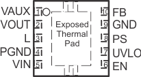
7 Pin Configuration and Functions

DSC and DRC Package
10 Pins
Top View
pino_lvs577.gif

Pin Functions

PIN I/O DESCRIPTION
NAME NO.
EN 6 I Enable input (High = enabled, Low = disabled). Do not leave floating.
Exposed thermal pad Must be soldered to achieve appropriate power dissipation and mechanical reliability. Should be connected to PGND.
FB 10 I Voltage feedback of adjustable versions, must be connected to VOUT at fixed output voltage versions
GND 9 Control / logic ground
PGND 4 Power ground
PS 8 I Enable/disable Power Save mode (High = disabled, Low = enabled). Do not leave floating.
L 3 I Connection for Inductor
UVLO 7 I Undervoltage lockout comparator input. Must be connected to VAUX if not used
VAUX 1 I/O Supply voltage for control stage
VIN 5 I Boost converter input voltage
VOUT 2 O Boost converter output