SLVS577E March 2007 – December 2014 TPS61200 , TPS61201 , TPS61202
PRODUCTION DATA.
- 1 Features
- 2 Applications
- 3 Description
- 4 Typical Application
- 5 Revision History
- 6 Device Options
- 7 Pin Configuration and Functions
- 8 Specifications
- 9 Parameter Measurement Information
- 10Detailed Description
- 11Application and Implementation
- 12Power Supply Recommendations
- 13Layout
- 14Device and Documentation Support
- 15Mechanical, Packaging, and Orderable Information
Package Options
Mechanical Data (Package|Pins)
- DRC|10
Thermal pad, mechanical data (Package|Pins)
- DRC|10
Orderable Information
8 Specifications
8.1 Absolute Maximum Ratings
over operating free-air temperature range (unless otherwise noted)(1)| MIN | MAX | UNIT | ||
|---|---|---|---|---|
| VIN | Input voltage range on VIN, L, VAUX, VOUT, PS, EN, FB, UVLO | –0.3 | 7 | V |
| TJ | Operating junction temperature | –40 | 150 | °C |
| Tstg | Storage temperature | –65 | 150 | °C |
(1) Stresses beyond those listed under Absolute Maximum Ratings may cause permanent damage to the device. These are stress ratings only, and functional operation of the device at these or any other conditions beyond those indicated under Recommended Operating Conditions is not implied. Exposure to absolute-maximum-rated conditions for extended periods may affect device reliability.
8.2 ESD Ratings
| VALUE | UNIT | |||
|---|---|---|---|---|
| V(ESD) | Electrostatic discharge | Human-body model (HBM), per ANSI/ESDA/JEDEC JS-001(1) | ±4000 | V |
| Charged-device model (CDM), per JEDEC specification JESD22-C101(2) | ±1500 | |||
| Machine Model (MM)(3) | ±200 | |||
(1) JEDEC document JEP155 states that 500-V HBM allows safe manufacturing with a standard ESD control process. Manufacturing with less than 500-V HBM is possible with the necessary precautions.
(2) JEDEC document JEP157 states that 250-V CDM allows safe manufacturing with a standard ESD control process. Manufacturing with less than 250-V CDM is possible with the necessary precautions.
(3) ESD testing is performed according to the respective JESD22 JEDEC standard.
8.3 Recommended Operating Conditions
| MIN | NOM | MAX | UNIT | ||
|---|---|---|---|---|---|
| VIN | Input voltage at VIN | 0.3 | 5.5 | V | |
| TA | Operating free air temperature range | –40 | 85 | °C | |
| TJ | Operating junction temperature range | –40 | 125 | °C | |
8.4 Thermal Information
| THERMAL METRIC(1) | TPS6120x | UNIT | ||
|---|---|---|---|---|
| DRC | DSC | |||
| 10 PINS | 10 PINS | |||
| RθJA | Junction-to-ambient thermal resistance | 41.2 | 40.4 | °C/W |
| RθJC(top) | Junction-to-case (top) thermal resistance | 62.8 | 37.8 | |
| RθJB | Junction-to-board thermal resistance | 16.6 | 15.4 | |
| ψJT | Junction-to-top characterization parameter | 1.2 | 0.3 | |
| ψJB | Junction-to-board characterization parameter | 16.8 | 15.6 | |
| RθJC(bot) | Junction-to-case (bottom) thermal resistance | 4.1 | 2.8 | |
(1) For more information about traditional and new thermal metrics, see the IC Package Thermal Metrics application report, SPRA953.
8.5 Electrical Characteristics
over recommended junction temperature range and over recommended input voltage range (typical at an ambient temperature range of 25°C) (unless otherwise noted)| PARAMETER | TEST CONDITIONS | MIN | TYP | MAX | UNIT | ||
|---|---|---|---|---|---|---|---|
| DC-DC STAGE | |||||||
| VIN | Input voltage range | 0.3 | 5.5 | V | |||
| VIN | Minimum input voltage at startup | 0.5 | V | ||||
| VOUT | TPS61200 output voltage range | 1.8 | 5.5 | V | |||
| VFB | TPS61200 feedback voltage | 495 | 500 | 505 | mV | ||
| VOUT | TPS61201 output voltage | VIN < VOUT, PS = High | 3.27 | 3.3 | 3.33 | V | |
| VOUT | TPS61202 output voltage | VIN < VOUT, PS = High | 4.95 | 5.0 | 5.05 | V | |
| f | Oscillator frequency | 1250 | 1650 | kHz | |||
| ILIM | average inductor current limit | VOUT = 3.3 V | 1200 | 1350 | 1500 | mA | |
| RDS(on) | Rectifying switch on resistance | VOUT = 3.3 V | 180 | mΩ | |||
| RDS(on) | Main switch on resistance | VOUT = 3.3 V | 150 | mΩ | |||
| Line regulation | VIN < VOUT, PS = High | 0.1% | 0.5% | ||||
| Load regulation | VIN < VOUT, PS = High | 0.1% | 0.5% | ||||
| IQ | Quiescent current | VIN | IO = 0 mA, VEN = VIN = 1.2 V, VOUT = 3.3 V, VAUX = 3.3 V PS = Low |
1 | 2 | μA | |
| VOUT | 50 | 70 | μA | ||||
| VAUX | 4 | 6 | μA | ||||
| ISD | Shutdown current | VIN | VEN = 0 V, VIN = 1.2 V | 0.5 | 1.5 | μA | |
| VAUX | 1 | 2 | μA | ||||
| ILKG | Input leakage current ( L) | VEN = 0 V, VIN = 1.2 V, VL = 1.2 V | 0.01 | 1 | μA | ||
| CONTROL STAGE | |||||||
| VAUX | Auxiliary Output Voltage | 2.4 | 5.5 | V | |||
| VIL | Low level input threshold voltage (EN) | VIN < 0.8 V | 0.1 × VIN | V | |||
| VIH | High level input threshold voltage (EN) | VIN < 0.8 V | 0.9 × VIN | V | |||
| VIL | Low level input threshold voltage (EN) | 0.8 V ≤ VIN ≤ 1.5 V | 0.2 × VIN | V | |||
| VIH | High level input threshold voltage (EN) | 0.8 V ≤ VIN ≤ 1.5 V | 0.8 × VIN | V | |||
| VIL | Low level input threshold voltage (EN) | VIN > 1.5 V | 0.4 | V | |||
| VIH | High level input threshold voltage (EN) | VIN > 1.5 V | 1.2 | V | |||
| VIL | Low level input threshold voltage (PS) | 0.4 | V | ||||
| VIH | High level input threshold voltage (PS) | 1.2 | V | ||||
| ILKG | Input leakage current (EN, PS) | EN, PS = GND or VIN | 0.01 | 0.1 | μA | ||
| VUVLO | Undervoltage lockout threshold | Falling UVLO voltage | 235 | 250 | 265 | mV | |
| VUVLO | Undervoltage lockout threshold | Rising UVLO voltage | 330 | 350 | 370 | mV | |
| ILKG | Input leakage current (UVLO) | VUVLO = 0.5 V | 0.3 | μA | |||
| VOVP | Overvoltage protection threshold | 5.5 | 7 | V | |||
| Thermal shutdown temperature | Rising temperature | 140 | °C | ||||
| Thermal shutdown temperature hysteresis | 20 | °C | |||||
8.6 Typical Characteristics
Table 1. Table of Graphs
| FIGURE | |||
|---|---|---|---|
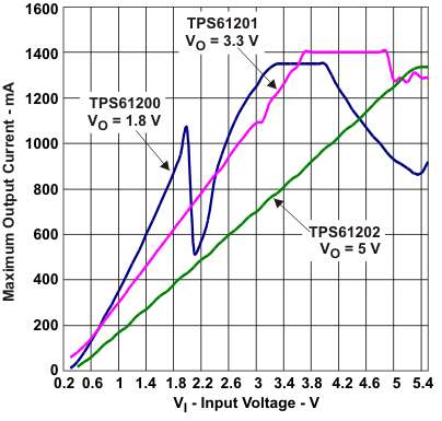
| Maximum output current | vs Input voltage | Figure 1 | |
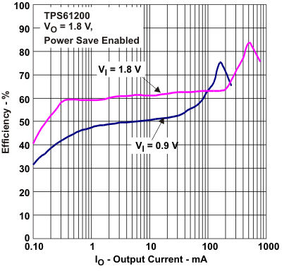
| Efficiency | vs Output current (TPS61200), Power Save Enabled | Figure 2 | |
| vs Output current (TPS61200), Power Save Disabled | Figure 3 | ||
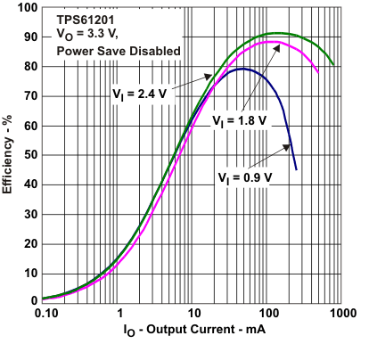
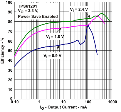
| vs Output current (TPS61201), Power Save Enabled | Figure 4 | ||
| vs Output current (TPS61201), Power Save Disabled | Figure 5 | ||
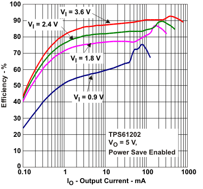
| vs Output current (TPS61202), Power Save Enabled | Figure 6 | ||
| vs Output current (TPS61202), Power Save Disabled | Figure 7 | ||
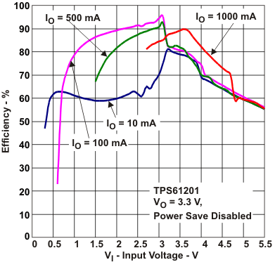
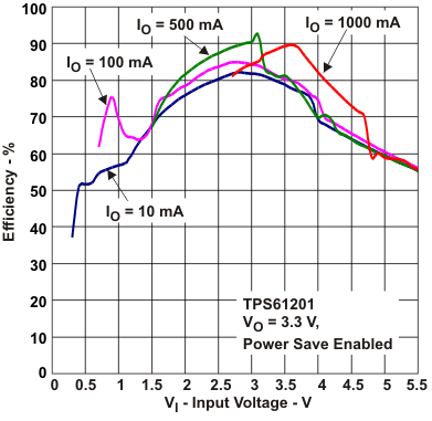
| vs Input voltage (TPS61201), Power Save Enabled | Figure 8 | ||
| vs Input voltage (TPS61201), Power Save Disabled | Figure 9 | ||
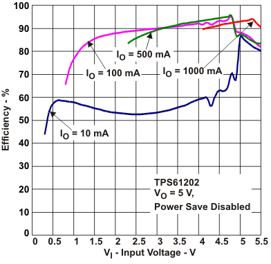
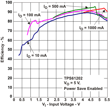
| vs Input voltage (TPS61202), Power Save Enabled | Figure 10 | ||
| vs Input voltage (TPS61202), Power Save Disabled | Figure 11 | ||
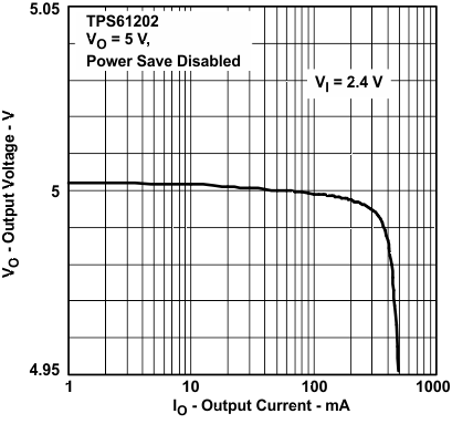
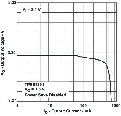
| Output voltage | vs Output current (TPS61201) | Figure 12 | |
| vs Output current (TPS61202) | Figure 13 | ||