SLVSC55C August 2013 – November 2021 TPS62090-Q1
PRODUCTION DATA
- 1 Features
- 2 Applications
- 3 Description
- 4 Revision History
- 5 Pin Configuration and Functions
- 6 Specifications
-
7 Detailed Description
- 7.1 Overview
- 7.2 Functional Block Diagram
- 7.3
Feature Description
- 7.3.1 Enable and Disable (EN)
- 7.3.2 Soft Start (SS) and Hiccup Current Limit During Start-Up
- 7.3.3 Voltage Tracking (SS)
- 7.3.4 Short-Circuit Protection (Hiccup Mode)
- 7.3.5 Output Discharge Function
- 7.3.6 Power Good Output (PG)
- 7.3.7 Frequency Set Pin (FREQ)
- 7.3.8 Undervoltage Lockout (UVLO)
- 7.3.9 Thermal Shutdown
- 7.3.10 Charge Pump (CP, CN)
- 7.4 Device Functional Modes
- 8 Application and Implementation
- 9 Power Supply Recommendations
- 10Layout
- 11Device and Documentation Support
- 12Mechanical, Packaging, and Orderable Information
Package Options
Mechanical Data (Package|Pins)
- RGT|16
Thermal pad, mechanical data (Package|Pins)
- RGT|16
Orderable Information
3 Description
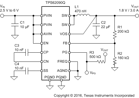
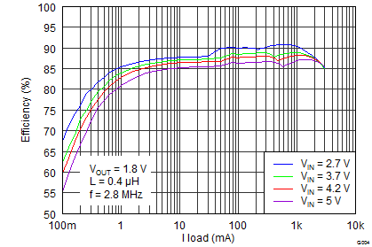
The TPS62090Q devices are a family of high-frequency, synchronous, step-down converters optimized for small solution size, high efficiency, and are suitable for battery-powered applications. To maximize efficiency, the converters operate in pulse width modulation (PWM) mode with a nominal switching frequency of 2.8 MHz to 1.4 MHz and automatically enter power save mode operation at light load currents. When used in distributed power supplies and point-of-load regulation, the devices allow voltage tracking to other voltage rails and tolerate output capacitors ranging from 10 µF up to 150 µF and beyond. Using the DCS-Control™ topology, the devices achieve excellent load transient performance and accurate output voltage regulation.
The output voltage start-up ramp is controlled by the SS pin, which allows operation as either a standalone power supply or in tracking configurations. Power sequencing is also possible by configuring the enable and power good pins. In power save mode, the devices operate at typically 20-µA quiescent current. Power save mode is entered automatically and seamlessly maintaining high efficiency over the entire load current range.
| PART NUMBER | PACKAGE(1) | BODY SIZE (NOM) |
|---|---|---|
| TPS62090Q | QFN (16) | 3.00 mm × 3.00 mm |
 Typical Application
 Efficiency