SLVSC55C August 2013 – November 2021 TPS62090-Q1
PRODUCTION DATA
- 1 Features
- 2 Applications
- 3 Description
- 4 Revision History
- 5 Pin Configuration and Functions
- 6 Specifications
-
7 Detailed Description
- 7.1 Overview
- 7.2 Functional Block Diagram
- 7.3
Feature Description
- 7.3.1 Enable and Disable (EN)
- 7.3.2 Soft Start (SS) and Hiccup Current Limit During Start-Up
- 7.3.3 Voltage Tracking (SS)
- 7.3.4 Short-Circuit Protection (Hiccup Mode)
- 7.3.5 Output Discharge Function
- 7.3.6 Power Good Output (PG)
- 7.3.7 Frequency Set Pin (FREQ)
- 7.3.8 Undervoltage Lockout (UVLO)
- 7.3.9 Thermal Shutdown
- 7.3.10 Charge Pump (CP, CN)
- 7.4 Device Functional Modes
- 8 Application and Implementation
- 9 Power Supply Recommendations
- 10Layout
- 11Device and Documentation Support
- 12Mechanical, Packaging, and Orderable Information
Package Options
Mechanical Data (Package|Pins)
- RGT|16
Thermal pad, mechanical data (Package|Pins)
- RGT|16
Orderable Information
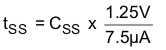
7.3.2 Soft Start (SS) and Hiccup Current Limit During Start-Up
To minimize inrush current during start-up, the device has an adjustable soft start depending on the capacitor value connected to the SS pin. The device charges the soft-start capacitor with a constant current of typically
7.5 µA. The feedback voltage follows this voltage with a fraction of 1.56 until the internal reference voltage of 0.8 V is reached. The soft-start operation is complete when the voltage at the soft-start capacitor has reached typically 1.25 V. The soft-start time is calculated using Equation 1. The larger the soft-start capacitor, the longer the soft-start time. The relation between soft-start voltage and feedback voltage is estimated using Equation 2.

During start-up, the switch current limit is reduced to 1/3 (approximately 1.5 A) of its typical current limit of 4.6 A. Once the output voltage exceeds typically 0.6 V, the current limit is released to its nominal value. The device provides a reduced load current of approximately 1.5 A when the output voltage is below typically 0.6 V. Due to this, a small or no soft-start time may trigger the short-circuit protection during start-up especially for larger output capacitors. This is avoided by using a larger soft-start capacitance to extend the soft-start time. See Section 7.3.4 for details of the reduced current limit during start-up. Leaving the soft-start pin floating sets the minimum start-up time (around 50 µs).