SLVSFP4B August 2020 – March 2021 TPS62912 , TPS62913
PRODUCTION DATA
- 1 Features
- 2 Applications
- 3 Description
- 4 Revision History
- 5 Pin Configuration and Functions
- 6 Specifications
-
7 Detailed Description
- 7.1 Overview
- 7.2 Functional Block Diagram
- 7.3
Feature Description
- 7.3.1 Smart Config (S-CONF)
- 7.3.2 Device Enable (EN/SYNC)
- 7.3.3 Device Synchronization (EN/SYNC)
- 7.3.4 Spread Spectrum Modulation
- 7.3.5 Output Discharge
- 7.3.6 Undervoltage Lockout (UVLO)
- 7.3.7 Power-Good Output
- 7.3.8 Noise Reduction and Soft-Start Capacitor (NR/SS)
- 7.3.9 Current Limit and Short Circuit Protection
- 7.3.10 Thermal Shutdown
- 7.4 Device Functional Modes
- 8 Application and Implementation
- 9 Power Supply Recommendations
- 10Layout
- 11Device and Documentation Support
- 12Mechanical, Packaging, and Orderable Information
Package Options
Mechanical Data (Package|Pins)
- RPU|10
Thermal pad, mechanical data (Package|Pins)
Orderable Information
8.2.2.2.2 Inductor Selection for the First L-C Filter
The inductor selection is dependent on the selected switching frequency and the duty cycle. When using the 2.2-MHz frequency, only use a 2.2-µH inductor. When using the 1-MHz frequency, calculate the maximum duty cycle using the minimum input voltage. If Dmax is above 45%, only use a 4.7-µH inductor. If Dmax is below 45% and the output voltage is 2 V or less, use only a 2.2-µH inductor. If Dmax is below 45% and the output voltage is above 2 V, use a 4.7-µH inductor to achieve the full output current or a 2.2-µH inductor for higher efficiency with a reduced maximum output current.
The inductor also has to be rated for the appropriate saturation current. Equation 5 and Equation 6 calculate the maximum inductor current under static load conditions. The formula takes the converter efficiency into account. The calculation must be done for the maximum input voltage where the peak switch current is highest.
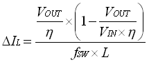
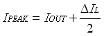
where
- ƒSW is the switching frequency (typically 1 MHz or 2.2 MHz)
- L is inductance
- η is estimated efficiency (use the value from the efficiency curves or 0.9 as an conservative assumption)
Calculating the maximum inductor current using the actual operating conditions gives the minimum saturation current. A margin of 20% is recommended to be added to cover for load transients during operation.
See Table 8-4 for typical inductors.
| INDUCTOR VALUE | MANUFACTURER | PART NUMBER | SIZE (L X W X H IN mm) | ISAT/DCR (30% DROP) |
|---|---|---|---|---|
| 2.2 µH | Coilcraft | XGL4020-222 | 4 × 4 × 2.1 | 6.2 A / 19.5 mΩ |
| 2.2 µH | Coilcraft | XGL4030-222 | 4 × 4 × 3.1 | 7 A / 13.5 mΩ |
| 2.2 µH | Wurth Elektronik | 74438356022 | 4.1 × 4.1 × 2.1 | 5.2 A / 35 mΩ |
| 2.2 µH | Wurth Elektronik | 74438357022 | 4.1 × 4.1 × 3.1 | 7 A / 26 mΩ |
| 2.2 µH | MuRata | DFE322520FD-2R2M=P2 | 3.2 × 2.5 × 2 | 5 A / 46 mΩ |
| 4.7 µH | Coilcraft | XGL4020-472 | 4 × 4 × 2.1 | 4.1 A / 43.0 mΩ |
| 4.7 µH | Coilcraft | XGL4030-472 | 4 × 4 × 3.1 | 4.4 A / 28.5 mΩ |
| 4.7 µH for TPS62912 only | MuRata | DFE322520FD-4R7M=P2 | 3.2 × 2.5 × 2 | 3.4 A / 98 mΩ |