SLVSA92C November 2011 – September 2020 TPS63060 , TPS63061
PRODUCTION DATA
- 1 Features
- 2 Applications
- 3 Description
- 4 Revision History
- 5 Device Comparison
- 6 Pin Configuration and Functions
- 7 Specifications
- 8 Detailed Description
- 9 Application and Implementation
- 10Power Supply Recommendations
- 11Layout
- 12Device and Documentation Support
- 13Mechanical, Packaging, and Orderable Information
Package Options
Mechanical Data (Package|Pins)
- DSC|10
Thermal pad, mechanical data (Package|Pins)
- DSC|10
Orderable Information
9.2.2.2 Step Two: Inductor Selection
The inductor selection is affected by several parameters including inductor ripple current, output voltage ripple, transition point into power-save mode, and efficiency. See Table 9-3 for typical inductors.
| Inductor Value (µH) | Component Suplier(1) | Size (L×W×H) (mm) | Current Saturation (ISAT) (A) | DCR (mΩ) |
|---|---|---|---|---|
| 1 | Coilcraft XFL4020-102 | 4 × 4 × 2.1 | 5.1 | 10.8 |
| 1 | TOKO DEM2815 1226AS-H-1R0N | 3 × 3.2 × 1.5 | 2.7 | 27 |
| 1.5 | Coilcraft XFL4020-152 | 4 × 4 × 2.1 | 4.4 | 14.4 |
For high efficiencies, the inductor should have a low dc resistance to minimize conduction losses. Especially at high-switching frequencies the core material has a higher impact on efficiency. When using small chip inductors, the efficiency is reduced mainly due to higher inductor core losses. This needs to be considered when selecting the appropriate inductor. The inductor value determines the inductor ripple current. The larger the inductor value, the smaller the inductor ripple current and the lower the conduction losses of the converter. Conversely, larger inductor values cause a slower load transient response. To avoid saturation of the inductor, with the chosen inductance value, the peak current for the inductor in steady state operation can be calculated. Equation 1 and Equation 5 show how to calculate the peak current IPEAK. Only the equation which defines the switch current in boost mode is reported because this is providing the highest value of current and represents the critical current value for selecting the right inductor.
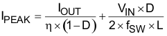
where
- D is the duty cycle during boost mode operation
- fSW is the converter switching frequency (typical 2.4 MHz)
- L is the selected inductor value
- η is the estimated converter efficiency (use the number from the efficiency curves or 0.80 as an assumption)
- The calculation must be done for the minimum input voltage which is possible to have in boost mode
Calculating the maximum inductor current using the actual operating conditions gives the minimum saturation current of the inductor needed. It's recommended to choose an inductor with a saturation current 20% higher than the value calculated using Equation 5. Possible inductors are listed in Table 9-3.