SLVSB04A July 2011 – August 2015 TPS65186
PRODUCTION DATA.
- 1 Features
- 2 Applications
- 3 Description
- 4 Revision History
- 5 Description (continued)
- 6 Pin Configuration and Functions
- 7 Specifications
-
8 Detailed Description
- 8.1 Overview
- 8.2 Functional Block Diagram
- 8.3 Feature Description
- 8.4 Device Functional Modes
- 8.5 Programming
- 8.6
Register Maps
- 8.6.1 Thermistor Readout (TMST_VALUE)
- 8.6.2 Enable (ENABLE)
- 8.6.3 Voltage Adjustment Register (VADJ)
- 8.6.4 VCOM 1 (VCOM1)
- 8.6.5 VCOM 2 (VCOM2)
- 8.6.6 Interrupt Enable 1 (INT_EN1)
- 8.6.7 Interrupt Enable 2 (INT_EN2)
- 8.6.8 Interrupt 1 (INT1)
- 8.6.9 Interrupt 2 (INT2)
- 8.6.10 Power Up Sequence Register 0 (UPSEQ0)
- 8.6.11 Power Up Sequence Register 1 (UPSEQ1)
- 8.6.12 Power Down Sequence Register 0 (DWNSEQ0)
- 8.6.13 Power Down Sequence Register 1 (DWNSEQ1)
- 8.6.14 Thermistor Register 1 (TMST1)
- 8.6.15 Thermistor Register 2 (TMST2)
- 8.6.16 Power Good Status (PG)
- 8.6.17 Revision and Version Control (REVID)
- 9 Application and Implementation
- 10Power Supply Recommendations
- 11Layout
- 12Device and Documentation Support
- 13Mechanical, Packaging, and Orderable Information
Package Options
Mechanical Data (Package|Pins)
- RGZ|48
Thermal pad, mechanical data (Package|Pins)
- RGZ|48
Orderable Information
9 Application and Implementation
NOTE
Information in the following applications sections is not part of the TI component specification, and TI does not warrant its accuracy or completeness. TI’s customers are responsible for determining suitability of components for their purposes. Customers should validate and test their design implementation to confirm system functionality.
9.1 Application Information
The TPS65186 is used to power display screens in E-book applications, specifically E-Ink Vizplex display, by connecting the screen to the positive and negative charge pump, LDOs 1 and 2, and VCOM rails. The display screens size that can be supported up to 9.7 inches.
9.2 Typical Application
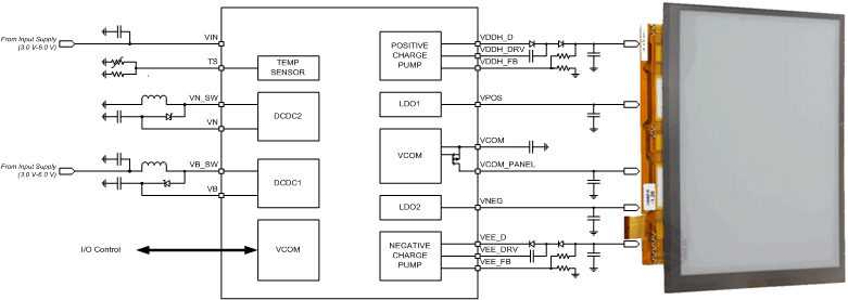
9.2.1 Design Requirements
For this design example, use the parameters listed in Table 2 as the input parameters.
Table 2. Design Parameters
| VOLTAGE | SEQUENCE (STROBE) | |
|---|---|---|
| VNEG (LDO2) | –15 V | 1 |
| VEE (Charge pump 2) | –20 V | 2 |
| VPOS (LDO1) | 15 V | 3 |
| VDDH (Charge pump 1) | 22 V | 4 |
9.2.2 Detailed Design Procedure
Table 3. Recommended External Components
| PART NUMBER | VALUE | SIZE | MANUFACTURER |
|---|---|---|---|
| INDUCTORS | |||
| LQH44PN4R7MP0 | 4.7 µH | 4 mm × 4 mm × 1.65 mm | Murata |
| NR4018T4R7M | 4.7 µH | 4 mm × 4 mm × 1.8 mm | Taiyo Yuden |
| VLS252015ET-2R2M | 2.2 µH | 2 mm × 2.5 mm × 1.5 mm | TDK |
| NR4012T2R2M | 2.2 µH | 4 mm × 4 mm × 1.2 mm | Taiyo Yuden |
| CAPACITORS | |||
| GRM21BC81E475KA12L | 4.7 µF, 25 V, X6S | 805 | Murata |
| GRM32ER71H475KA88L | 4.7 µF, 50 V, X7R | 1210 | Murata |
| All other capacitors | X5R or better | — | — |
| DIODES | |||
| BAS3010 | — | SOD-323 | Infineon |
| MBR130T1 | — | SOD-123 | ON-Semi |
| BAV99 | — | SOT-23 | Fairchild |
| THERMISTOR | |||
| NCP18XH103F03RB | 10 kΩ | 603 | Murata |
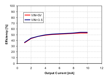
9.2.3 Application Curves
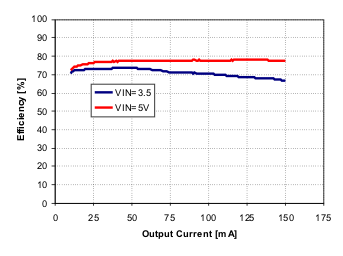
| T = 25°C |
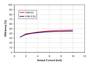
| T = 25°C |
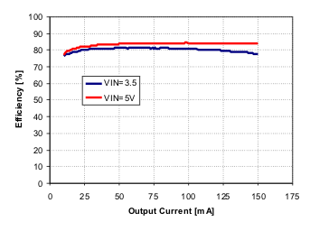
| T = 25°C |
| T = 25°C |