SLVSB04A July 2011 – August 2015 TPS65186
PRODUCTION DATA.
- 1 Features
- 2 Applications
- 3 Description
- 4 Revision History
- 5 Description (continued)
- 6 Pin Configuration and Functions
- 7 Specifications
-
8 Detailed Description
- 8.1 Overview
- 8.2 Functional Block Diagram
- 8.3 Feature Description
- 8.4 Device Functional Modes
- 8.5 Programming
- 8.6
Register Maps
- 8.6.1 Thermistor Readout (TMST_VALUE)
- 8.6.2 Enable (ENABLE)
- 8.6.3 Voltage Adjustment Register (VADJ)
- 8.6.4 VCOM 1 (VCOM1)
- 8.6.5 VCOM 2 (VCOM2)
- 8.6.6 Interrupt Enable 1 (INT_EN1)
- 8.6.7 Interrupt Enable 2 (INT_EN2)
- 8.6.8 Interrupt 1 (INT1)
- 8.6.9 Interrupt 2 (INT2)
- 8.6.10 Power Up Sequence Register 0 (UPSEQ0)
- 8.6.11 Power Up Sequence Register 1 (UPSEQ1)
- 8.6.12 Power Down Sequence Register 0 (DWNSEQ0)
- 8.6.13 Power Down Sequence Register 1 (DWNSEQ1)
- 8.6.14 Thermistor Register 1 (TMST1)
- 8.6.15 Thermistor Register 2 (TMST2)
- 8.6.16 Power Good Status (PG)
- 8.6.17 Revision and Version Control (REVID)
- 9 Application and Implementation
- 10Power Supply Recommendations
- 11Layout
- 12Device and Documentation Support
- 13Mechanical, Packaging, and Orderable Information
Package Options
Mechanical Data (Package|Pins)
- RGZ|48
Thermal pad, mechanical data (Package|Pins)
- RGZ|48
Orderable Information
11 Layout
11.1 Layout Guidelines
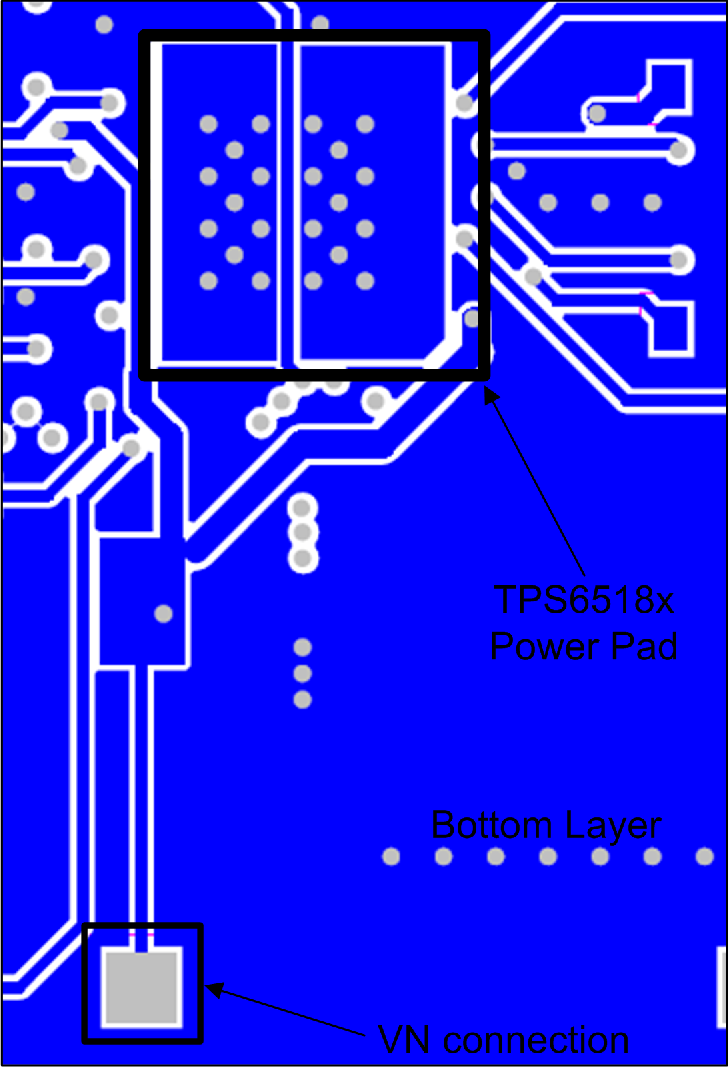
- PBKG (Die substrate) must connect to VN (–16 V) with short, wide trace. Wide copper trace will improve heat dissipation.
- PowerPad is internally connected to PBKG and must not be connected to ground, but connected to VN with a short wide copper trace.
- Inductor traces must be kept on the PCB top layer free of any vias.
- Feedback traces must be routed away from any potential noise source to avoid coupling.
- Output caps must be placed immediately at output pin.
- Vin pins must be bypassed to ground with low ESR ceramic bypass capacitors.
11.2 Layout Example
 Figure 33. Layout Diagram