Over operating temperature range (TJ = –40°C to 125°C), IOUT = 10 mA, VEN = 2 V, COUT = 2.2 μF, and VIN = VOUT(nom) + 1 V or 2.7 V (whichever is greater), unless otherwise noted. Typical values are at TJ = 25°C.
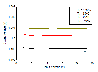
 Figure 5-1 1.2-V Line Regulation vs VIN and Temperature
 Figure 5-3 6.5-V Line Regulation vs VIN and Temperature
 Figure 5-5 3.3-V Load Regulation vs IOUT and Temperature
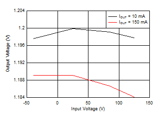
 Figure 5-7 1.2-V Output Voltage vs Temperature
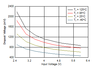
 Figure 5-9 3.3-V Dropout Voltage vs IOUT and Temperature
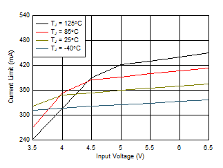
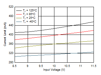
 Figure 5-11 1.2-V Current Limit vs VIN and Temperature
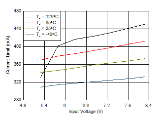
 Figure 5-13 6.5-V Current Limit vs VIN and Temperature
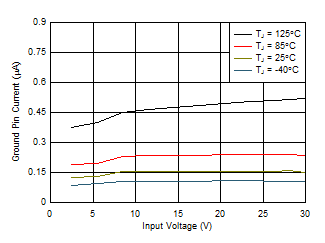
 Figure 5-15 3.3-V Ground Pin Current vs VIN and Temperature
 Figure 5-17 3.3-V Ground Current vs VIN and Temperature with EN Floating
 Figure 5-19 3.3-V Ground Pin Current vs IOUT and Temperature
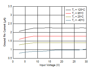
 Figure 5-21 1.2-V Shutdown Current vs VIN and Temperature
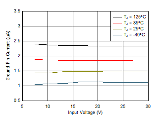
 Figure 5-23 6.5-V Shutdown Current vs VIN and Temperature
 Figure 5-25 Power-Supply Rejection Ratio vs Frequency
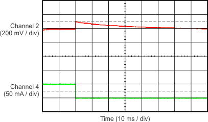
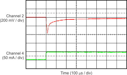
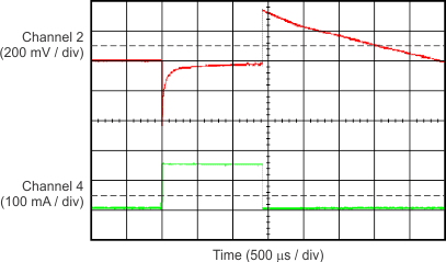
| Channel 2 = VOUT, channel 4 = IOUT, VIN = 2.7 V |

| Channel 2 = VOUT, channel 4 = IOUT, VIN = 2.7 V |

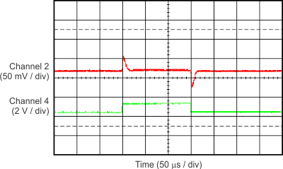
| Channel 2 = VOUT, channel 4 = IOUT, VIN = 4.3 V |

| Channel 2 = VOUT, channel 4 = IOUT, VIN = 4.3 V |

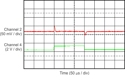
| Channel 2 = VOUT, channel 4 = VIN, IOUT = 10 mA |

| Channel 2 = VOUT, channel 4 = VIN, IOUT = 10 mA |

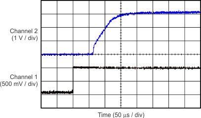
| Channel 1 = EN, channel 2 = VOUT, VIN = 4.3 V, COUT = 2.2 µF, TPS70633 |

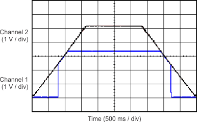
| Channel 1 = VIN, channel 2 = VOUT, IOUT = 150 mA, TPS70633 |
 Figure 5-2 3.3-V Line Regulation vs VIN and Temperature
 Figure 5-4 1.2-V Load Regulation vs IOUT and Temperature
 Figure 5-6 6.5-V Load Regulation vs IOUT and Temperature
 Figure 5-8 6.5-V Dropout Voltage vs VIN and Temperature
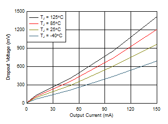
 Figure 5-10 Dropout Voltage vs IOUT and Temperature
 Figure 5-12 3.3-V Current Limit vs VIN and Temperature
 Figure 5-14 1.2-V Ground Pin Current vs VIN and Temperature
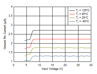
 Figure 5-16 6.5-V Ground Pin Current vs VIN and Temperature
 Figure 5-18 1.2-V Ground Pin Current vs IOUT and Temperature
 Figure 5-20 6.5-V Ground Pin Current vs IOUT and Temperature
 Figure 5-22 3.3-V Shutdown Current vs VIN and Temperature
 Figure 5-24 Start-Up Time vs Temperature
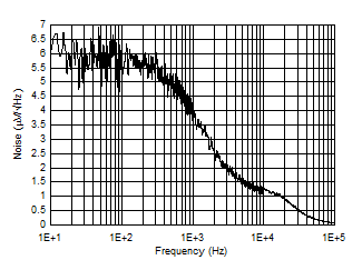
 Figure 5-26 Noise
| Channel 2 = VOUT, channel 4 = IOUT, VIN = 2.7 V |

| Channel 2 = VOUT, channel 4 = IOUT, VIN = 2.7 V |

| Channel 2 = VOUT, channel 4 = IOUT, VIN = 4.3 V |

| Channel 2 = VOUT, channel 4 = IOUT, VIN = 4.3 V |

| Channel 2 = VOUT, channel 4 = VIN, IOUT = 50 mA |

| Channel 2 = VOUT, channel 4 = VIN, IOUT = 50 mA |

| Channel 1 = VIN, channel 2 = VOUT, IOUT = 3 mA, TPS70633 |
| |
